Content Menu
● What Is SMT Stencil? — SMT Stencil Definition
● Why the SMT Stencil Definition Matters in High-Volume PCB Production
>> 1. Ensures Precision and Consistency in Solder Paste Application
>> 2. Enhances Production Efficiency and Throughput
>> 3. Supports Complex and High-Density PCB Designs
>> 4. Reduces Defects and Improves Product Quality
>> 5. Cost Savings Through Waste Reduction and Rework Minimization
● Types of SMT Stencils
● SMT Stencil Manufacturing Processes
● Benefits of Using Well-Defined SMT Stencils in High-Volume PCB Production
● Conclusion
● FAQ
>> 1. What is the primary function of an SMT stencil in PCB production?
>> 2. How does stencil thickness affect solder paste deposition?
>> 3. Why is laser cutting preferred for SMT stencil manufacturing?
>> 4. What are step stencils and why are they used?
>> 5. How do SMT stencils contribute to cost savings in PCB manufacturing?
● Citations:
In the fast-paced and precision-driven world of electronics manufacturing, the role of Surface Mount Technology (SMT) stencils is paramount, especially in high-volume printed circuit board (PCB) production. Understanding the SMT stencil definition and its implications is critical for manufacturers aiming to achieve high efficiency, quality, and reliability in their assembly processes. This article explores the importance of SMT stencils, their types, manufacturing processes, benefits, and how their precise definition impacts high-volume PCB production.

What Is SMT Stencil? — SMT Stencil Definition
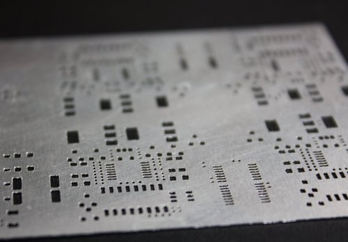
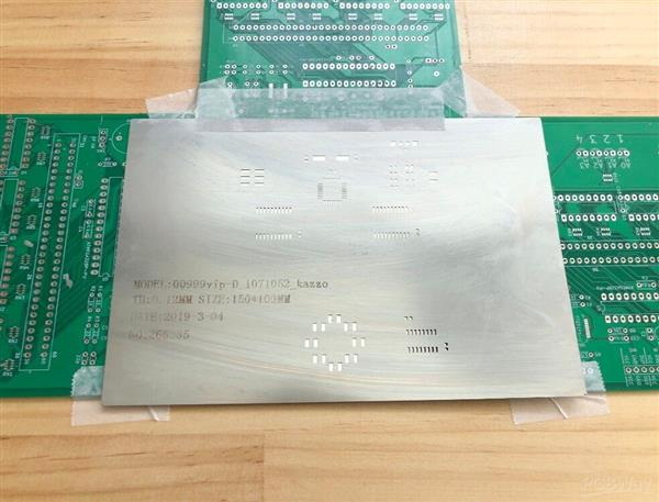
An SMT stencil, also known as a PCB stencil or solder paste stencil, is a thin sheet, typically made from stainless steel or nickel alloys, with laser-cut apertures that correspond to the solder pads on a PCB. Its primary function is to accurately deposit solder paste onto the PCB pads during the solder printing process, which is a crucial step in SMT assembly[1][3][4].
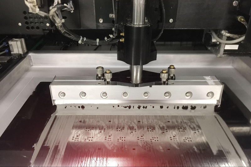
The stencil acts as a precise screening template, allowing solder paste to pass through the apertures and be deposited exactly where surface mount devices (SMDs) will be placed. This ensures a controlled volume of solder paste is applied, which is essential for forming reliable solder joints after reflow soldering[3][5].
Why the SMT Stencil Definition Matters in High-Volume PCB Production
1. Ensures Precision and Consistency in Solder Paste Application
The definition of an SMT stencil includes its material, thickness, aperture size, and aperture shape, all of which directly affect the volume and placement accuracy of solder paste. In high-volume PCB production, even minor deviations can lead to defects such as solder bridging, insufficient solder, or solder balls, which compromise the electrical and mechanical integrity of the PCB assembly[3][6][9].
A well-defined SMT stencil maintains tight tolerances in thickness (often within ±1%) and flatness, ensuring uniform paste deposition across thousands of boards. This consistency is critical for maintaining high yields and minimizing rework costs[9].
2. Enhances Production Efficiency and Throughput
High-volume PCB production demands rapid and repeatable processes. SMT stencils enable automated solder paste printing that is much faster and more reliable than manual application methods. The stencil definition governs how well the stencil fits on the PCB and how easily solder paste releases from the apertures, directly impacting cycle times and throughput[6][10].
By using stencils with precise aperture geometries and smooth aperture walls (achieved through advanced manufacturing techniques like laser cutting and electro-polishing), manufacturers can reduce printing defects and downtime, thus enhancing overall productivity[7][11].
3. Supports Complex and High-Density PCB Designs
Modern electronic devices often require PCBs with fine-pitch components and high-density layouts. The SMT stencil definition must accommodate these complexities by enabling apertures that match intricate pad geometries and varying solder paste volumes. Step stencils, which have variable thickness areas, are an example of how stencil design adapts to complex PCBs to ensure optimal solder paste deposition for different component types on the same board[5][11].
Without a precise stencil definition, achieving the required solder paste volume and placement accuracy on such complex boards would be nearly impossible, leading to assembly failures and increased production costs.
4. Reduces Defects and Improves Product Quality
The quality of solder joints is directly linked to the stencil's ability to deposit the correct amount of solder paste uniformly. A well-defined SMT stencil minimizes defects like tombstoning, misalignment, and solder bridging, which can cause functional failures in electronic devices[6][9][10].
Improved product quality translates into higher reliability, fewer field failures, and better customer satisfaction, which are vital for manufacturers competing in high-volume markets.
5. Cost Savings Through Waste Reduction and Rework Minimization
Using an SMT stencil with a precise definition reduces solder paste waste by controlling the exact amount of paste deposited. It also lowers the incidence of defects that require costly rework or scrap. Over large production runs, these savings become significant, improving profitability[6][9][10].
Types of SMT Stencils
Understanding the types of SMT stencils helps clarify how the stencil definition varies to meet different production needs:
- Frameless SMT Stencils: Flexible and cost-effective, ideal for prototypes or small batches. They adapt quickly to design changes but may lack the stability required for high-volume production[8].
- Framed SMT Stencils: Mounted on a rigid frame, these stencils provide stability and repeatability, making them suitable for high-volume manufacturing where consistent quality is essential[8].
- Prototype SMT Stencils: Used for rapid prototyping, enabling quick adjustments and testing of new PCB designs[8].
- Step Stencils: Feature areas of different thicknesses to deposit varying solder paste volumes on the same PCB, critical for complex assemblies[11].

SMT Stencil Manufacturing Processes
The manufacturing process affects the stencil definition and quality:
- Laser Cutting: The most common method, offering high precision (±4μm) and smooth aperture walls after polishing. It allows for complex aperture shapes suitable for fine-pitch components[7][11].
- Electroforming: An additive process producing nickel stencils with excellent surface finish and gasketing properties, ideal for ultra-fine pitch applications but more expensive and slower to produce[7][11].
- Chemical Etching: A subtractive process less precise than laser cutting, gradually being phased out due to environmental concerns and lower accuracy[7][11].
Benefits of Using Well-Defined SMT Stencils in High-Volume PCB Production
- Improved accuracy and consistency in solder paste deposition, leading to reliable solder joints[6].
- Increased efficiency and productivity by enabling faster, automated solder paste printing[6][10].
- Cost savings from reduced solder paste waste, fewer defects, and minimized rework[6][9].
- Enhanced product quality and reliability, resulting in higher yields and customer satisfaction[6][9].
- Capability to handle complex, high-density PCB designs with fine-pitch components[5][11].
Conclusion
The SMT stencil definition is a foundational element in high-volume PCB production, influencing every aspect of the solder paste printing process. From material selection and aperture design to manufacturing precision and flatness control, the stencil's characteristics determine the quality, efficiency, and cost-effectiveness of SMT assembly.
In high-volume environments, where speed and reliability are paramount, a well-defined SMT stencil ensures consistent solder paste deposition, reduces defects, supports complex PCB designs, and ultimately leads to superior product quality and profitability. As PCB technology advances, the importance of precise SMT stencil definition will only grow, making it an indispensable focus for electronics manufacturers.

FAQ
1. What is the primary function of an SMT stencil in PCB production?
An SMT stencil serves as a precise template to apply solder paste onto PCB pads, ensuring accurate and consistent solder paste deposition for reliable solder joints[1][3][4].
2. How does stencil thickness affect solder paste deposition?
Stencil thickness controls the volume of solder paste deposited on each pad. Tight thickness tolerances (often ±1%) ensure consistent paste volume, which is critical for solder joint quality and assembly reliability[9].
3. Why is laser cutting preferred for SMT stencil manufacturing?
Laser cutting offers high precision, smooth aperture walls, and the ability to create complex aperture shapes, making it ideal for fine-pitch and high-density PCB assemblies[7][11].
4. What are step stencils and why are they used?
Step stencils have areas of different thicknesses to deposit varying amounts of solder paste on different parts of the same PCB, accommodating components with different soldering requirements[5][11].
5. How do SMT stencils contribute to cost savings in PCB manufacturing?
By ensuring precise solder paste application, SMT stencils reduce solder paste waste, minimize defects and rework, and increase production throughput, all of which lower overall manufacturing costs[6][9][10].
Citations:
[1] https://www.pcbonline.com/blog/pcb-stencil-introduction.html
[2] https://www.wevolver.com/article/pcb-stencil
[3] https://www.elepcb.com/blog/pcb-stencil-smt-assembly/
[4] https://www.keepbestpcba.com/pcb-stencil/
[5] https://www.rigiflex.com/blog/a-brief-introduction-to-smt-stencils-for-printed-circuit-boards/
[6] https://flexpcb.org/benefits-of-smt-stencil/
[7] https://www.stencilsunlimited.com/blog/stencil-manufacturing-technologies/
[8] https://jlcpcb.com/blog/guide-to-smt-stencils-in-pcb-assembly
[9] https://www.datumalloys.com/stencils-and-their-ultimate-influence/
[10] https://www.technotronix.us/smt-stencils.html
[11] https://www.aipcba.com/pcb/smt-stencil-fabrication.html
[12] https://jlcpcb.com/blog/why-pcb-stencils-are-key-to-high-quality-smt-assembly
[13] https://stencillaser.lpkf.com/en/technology/about-stencil-manufacturing
[14] https://www.7pcb.com/blog/stencil-technology-smt-production


