Content Menu
● Introduction to Custom SMT PCB Assembly
● Benefits of Custom SMT PCB Assembly for High-Volume Production
>> 1. Cost Efficiency
>> 2. High Precision
>> 3. Scalability
>> 4. Reduced Lead Times
>> 5. Enhanced Reliability
>> 6. Miniaturization
● Key Considerations in High-Volume Custom SMT PCB Assembly
>> 1. Design for Manufacturing (DFM)
>> 2. Material Selection
>> 3. Panelization
>> 4. Testing Protocols
>> 5. Supply Chain Management
● The Role of Automation in SMT PCB Assembly
>> 1. Pick-and-Place Machines
>> 2. Soldering Techniques
>> 3. Inspection Systems
>> 4. Material Handling Systems
● Challenges and Solutions in High-Volume Production
>> 1. Component Availability
>> 2. Defect Management
>> 3. Design Complexity
>> 4. Thermal Management
>> 5. Flexibility in Production
● Future Trends in Custom SMT PCB Assembly
>> 1. Industry 4.0 Integration
>> 2. Advanced Materials
>> 3. 3D Printed Electronics
>> 4. AI-Driven Design Optimization
>> 5. Sustainable Manufacturing
● Case Studies: Success Stories in High-Volume Production
>> Case Study 1: Consumer Electronics Manufacturer
>> Case Study 2: Automotive Electronics Supplier
● Conclusion
● FAQs
>> 1. What is custom SMT PCB assembly?
>> 2. Why is automation important in high-volume custom SMT PCB assembly?
>> 3. How does Design for Manufacturing (DFM) benefit custom SMT PCB assembly?
>> 4. What industries benefit most from custom SMT PCB assembly?
>> 5. What testing methods are used in high-volume custom SMT PCB assembly?
In the fast-paced electronics industry, custom SMT PCB assembly has emerged as a critical solution for high-volume production. This process combines the benefits of Surface Mount Technology (SMT) with tailored designs to meet specific production requirements. Whether you're a small business scaling up or a large enterprise optimizing efficiency, custom SMT PCB assembly offers unmatched precision, cost-effectiveness, and scalability.

Introduction to Custom SMT PCB Assembly
Surface Mount Technology (SMT) is a revolutionary method where components are directly mounted onto the surface of a printed circuit board (PCB). Unlike traditional through-hole technology, SMT eliminates the need for drilling holes, enabling faster and more compact assembly processes.
When applied to custom high-volume production, SMT PCB assembly becomes even more powerful. It allows manufacturers to design PCBs tailored to specific applications, ensuring optimized performance and reliability in mass production scenarios. This customization is particularly beneficial for industries like consumer electronics, automotive, telecommunications, and medical devices.
The evolution of custom SMT PCB assembly has been driven by the increasing demand for smaller, more complex electronic devices. As products become more sophisticated, the need for precise, efficient, and scalable manufacturing processes has never been greater. Custom SMT PCB assembly meets these challenges head-on, offering a flexible solution that can adapt to various production volumes and design complexities.
Benefits of Custom SMT PCB Assembly for High-Volume Production
Custom SMT PCB assembly offers several advantages that make it ideal for large-scale manufacturing:
1. Cost Efficiency
- Bulk sourcing of components reduces material costs significantly.
- Automated processes minimize labor expenses and errors.
- Economies of scale lead to lower per-unit costs in high-volume production.
2. High Precision
- Advanced pick-and-place machines ensure accurate component placement.
- Automated Optical Inspection (AOI) detects defects early in the process.
- Precise solder paste application improves connection reliability.
3. Scalability
- Custom designs can be easily scaled from prototypes to tens of thousands of units.
- Dedicated production lines optimize throughput for high-volume orders.
- Flexible manufacturing systems allow for quick adjustments to production volumes.
4. Reduced Lead Times
- Pre-sourced components and automated workflows accelerate production timelines.
- Quick turnaround ensures faster time-to-market for products.
- Efficient inventory management reduces delays in the supply chain.
5. Enhanced Reliability
- Rigorous testing protocols like solder paste inspection and functional circuit testing ensure quality.
- Custom designs reduce the risk of failures in specific applications.
- Improved thermal management through optimized component placement.
6. Miniaturization
- SMT allows for higher component density, enabling smaller PCB designs.
- Compact layouts support the trend towards smaller, more portable devices.
- Reduced board size often leads to lower material costs and improved performance.
Key Considerations in High-Volume Custom SMT PCB Assembly
To achieve optimal results, manufacturers must address several critical factors during custom SMT PCB assembly:
1. Design for Manufacturing (DFM)
Following DFM guidelines ensures that PCBs are optimized for automated assembly processes. This includes proper component spacing, orientation, and thermal management. DFM also considers factors like:
- Component selection for automated placement
- Solder pad design for optimal adhesion
- Trace width and spacing for reliable connections
2. Material Selection
Choosing high-quality components that meet industry standards (e.g., RoHS compliance) is essential for durability and performance. Considerations include:
- PCB substrate material for thermal and electrical properties
- Solder paste composition for reliable joints
- Component quality and sourcing from reputable suppliers
3. Panelization
For high-volume production, multiple PCBs are manufactured on a single panel to maximize efficiency and reduce waste. Effective panelization strategies involve:
- Optimizing panel size for production equipment
- Designing break-away tabs or V-scoring for easy separation
- Balancing panel density with handling requirements
4. Testing Protocols
Comprehensive testing methods like X-ray inspection and in-circuit testing are crucial to detect defects early and maintain quality standards. A robust testing strategy may include:
- Automated Optical Inspection (AOI) for surface defects
- X-ray inspection for hidden solder joint issues
- In-Circuit Testing (ICT) for electrical functionality
- Functional testing to simulate real-world conditions
5. Supply Chain Management
Efficient supply chain management is critical for maintaining consistent production in high-volume scenarios. Key aspects include:
- Building relationships with reliable component suppliers
- Implementing just-in-time inventory systems
- Developing contingency plans for potential supply disruptions

The Role of Automation in SMT PCB Assembly
Automation is the backbone of high-volume custom SMT PCB assembly. It enhances efficiency, accuracy, and consistency across all stages of production:
1. Pick-and-Place Machines
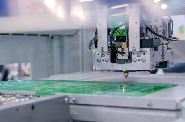
Automated machines place components with incredible speed and precision, reducing manual intervention and errors. Modern pick-and-place systems can:
- Handle components as small as 01005 (0.4mm x 0.2mm)
- Place up to 100,000 components per hour
- Adjust placement force for delicate components
2. Soldering Techniques
Jet solder paste printing and reflow soldering ensure strong electrical connections while maintaining high throughput rates. Advanced soldering technologies include:
- Stencil printing for precise solder paste application
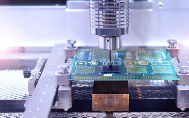
- Reflow ovens with multiple heating zones for optimal thermal profiles
- Selective soldering for mixed technology boards
3. Inspection Systems
Automated Optical Inspection (AOI) systems use advanced imaging techniques to identify defects in real-time, ensuring only flawless boards proceed to the next stage. Modern inspection systems feature:
- High-resolution cameras for detecting microscopic defects
- AI-powered defect recognition algorithms
- 3D inspection capabilities for solder joint quality assessment
4. Material Handling Systems
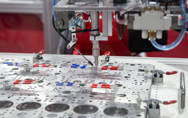
Automated conveyor systems and robotic handlers streamline the movement of PCBs through various production stages, reducing the risk of damage and improving efficiency.
Challenges and Solutions in High-Volume Production
Despite its advantages, high-volume custom SMT PCB assembly comes with challenges that require strategic solutions:
1. Component Availability
Challenge: Delays in sourcing components can disrupt production timelines.
Solution: Partnering with reliable suppliers ensures timely delivery of bulk materials. Additionally, implementing forecasting tools and maintaining safety stock levels can mitigate supply chain risks.
2. Defect Management
Challenge: A single defect can impact thousands of units.
Solution: Implementing stringent quality control measures like AOI and functional testing minimizes risks. Developing a comprehensive defect tracking and analysis system helps identify root causes and implement corrective actions quickly.
3. Design Complexity
Challenge: Complex designs may complicate assembly processes.
Solution: Simplifying layouts through Design for Assembly (DFA) principles improves manufacturability. Collaborating closely with design teams to optimize component placement and routing can significantly enhance production efficiency.
4. Thermal Management
Challenge: High-density designs can lead to heat dissipation issues.
Solution: Implementing thermal simulation during the design phase and incorporating heat sinks or thermal vias can improve heat management in densely packed PCBs.
5. Flexibility in Production
Challenge: Adapting to changes in product demand or design updates.
Solution: Investing in flexible manufacturing systems that can quickly switch between different product lines. Implementing modular production cells allows for easy reconfiguration based on changing requirements.
Future Trends in Custom SMT PCB Assembly
As technology continues to evolve, custom SMT PCB assembly is poised for further advancements:
1. Industry 4.0 Integration
The integration of IoT sensors and data analytics will enable predictive maintenance and real-time optimization of assembly processes.
2. Advanced Materials
Development of new PCB substrates and conductive materials will enhance performance and reliability in extreme conditions.
3. 3D Printed Electronics
Additive manufacturing techniques may complement traditional SMT assembly, allowing for more complex 3D circuit structures.
4. AI-Driven Design Optimization
Artificial intelligence algorithms will assist in creating more efficient PCB layouts and component placements, further optimizing the assembly process.
5. Sustainable Manufacturing
Increased focus on eco-friendly materials and energy-efficient production methods will drive innovation in sustainable SMT PCB assembly practices.
Case Studies: Success Stories in High-Volume Production
Case Study 1: Consumer Electronics Manufacturer
A leading smartphone manufacturer implemented custom SMT PCB assembly for their latest model, resulting in:
- 30% reduction in production time
- 15% decrease in material costs
- 50% improvement in defect detection rates
Case Study 2: Automotive Electronics Supplier
An automotive electronics supplier adopted advanced custom SMT PCB assembly techniques for their engine control units, achieving:
- 40% increase in production capacity
- 25% reduction in board size
- 99.9% first-pass yield rate
These case studies demonstrate the tangible benefits of investing in custom SMT PCB assembly for high-volume production across different industries.
Conclusion
Custom SMT PCB assembly is a game-changer for high-volume production, offering unparalleled efficiency, precision, and scalability. By leveraging automation, adhering to best practices like DFM, and addressing potential challenges proactively, manufacturers can achieve superior results while maintaining cost-effectiveness.
The future of custom SMT PCB assembly looks promising, with emerging technologies set to further enhance its capabilities. As industries continue to demand smaller, more complex electronic devices, the role of custom SMT PCB assembly in high-volume production will only grow in importance.
Whether you're producing consumer electronics or industrial equipment, investing in custom solutions tailored to your needs will help you stay competitive in today's dynamic market. By embracing the latest advancements in SMT technology and continuously optimizing your production processes, you can ensure that your high-volume PCB assembly operations remain at the cutting edge of efficiency and quality.

FAQs
1. What is custom SMT PCB assembly?
Custom SMT PCB assembly involves tailoring the design and manufacturing processes of printed circuit boards using Surface Mount Technology to meet specific requirements. This approach allows for optimized component placement, improved performance, and efficient high-volume production.
2. Why is automation important in high-volume custom SMT PCB assembly?
Automation enhances efficiency by reducing manual errors, speeding up processes like component placement and soldering, and ensuring consistent quality through automated inspections. It also enables manufacturers to handle large production volumes with greater precision and speed than manual assembly methods.
3. How does Design for Manufacturing (DFM) benefit custom SMT PCB assembly?
DFM ensures that PCBs are designed with manufacturing constraints in mind, improving yield rates, reducing costs, and minimizing defects during production. It considers factors such as component spacing, thermal management, and testability to create designs that are optimized for the assembly process.
4. What industries benefit most from custom SMT PCB assembly?
Industries such as consumer electronics, automotive, telecommunications, medical devices, and aerospace benefit significantly due to their demand for high precision and reliability. These sectors often require complex, high-density PCBs produced in large volumes, making custom SMT PCB assembly an ideal solution.
5. What testing methods are used in high-volume custom SMT PCB assembly?
Common methods include Automated Optical Inspection (AOI), X-ray inspection, solder paste inspection, functional circuit testing (FCT), and in-circuit testing (ICT). These techniques ensure that each PCB meets quality standards and functions correctly before final assembly into the end product.


