Content Menu
● What is a PCB?
>> PCB Materials and Construction
>> PCB Design Considerations
● What is an SMT Stencil?
>> How SMT Stencils Work
>> Types of SMT Stencils
>> Materials and Thickness
● Key Differences Between SMT Stencil and PCB
● Why Is the SMT Stencil Important in PCB Assembly?
>> Benefits of Using SMT Stencils
>> Impact on Assembly Yield and Reliability
● The Relationship Between SMT Stencil and PCB
>> Design Collaboration Between PCB and SMT Stencil
● Common Misconceptions About SMT Stencil vs PCB
● Advanced Considerations in SMT Stencil and PCB Interaction
>> Fine Pitch Components and Stencil Design
>> Solder Paste Types and Stencil Compatibility
>> Cleaning and Maintenance of SMT Stencils
● Conclusion
● FAQ
>> 1. What is the main function of an SMT stencil in PCB assembly?
>> 2. Can a PCB be assembled without using an SMT stencil?
>> 3. What materials are SMT stencils typically made from?
>> 4. How does the SMT stencil relate to the PCB design?
>> 5. What are the different types of SMT stencils?
In the world of electronics manufacturing, two terms that frequently come up are SMT stencil and PCB. While they are closely related and both essential to the assembly of electronic devices, they serve very different purposes. Understanding the difference between SMT stencil and PCB is crucial for anyone involved in electronics design, manufacturing, or assembly. This article provides a comprehensive explanation of what SMT stencils and PCBs are, how they work, their roles in the manufacturing process, and why both are indispensable in modern electronics production.

What is a PCB?
A Printed Circuit Board (PCB) is the foundational platform for most electronic devices. It is a laminated sandwich structure composed of conductive and insulating layers. The conductive layers, usually made of copper, are etched to form circuit traces and pads that electrically connect various electronic components. The insulating layers provide mechanical support and electrical isolation between the conductive paths.
PCBs come in various configurations:
- Single-sided PCBs have copper on one side only.
- Double-sided PCBs have copper layers on both sides.
- Multi-layer PCBs consist of multiple layers of copper and insulating material stacked together to allow for higher component density and complex circuits.
Components such as resistors, capacitors, integrated circuits, and connectors are mounted on the PCB, typically by soldering them to the copper pads.
PCBs are essential because they provide a reliable and compact way to interconnect components, enabling complex electronic functions in everything from smartphones to industrial machinery. The design of a PCB involves careful layout of traces and pads to ensure electrical performance and manufacturability.
PCB Materials and Construction
The most common material used for PCBs is FR-4, a fiberglass epoxy laminate that offers good mechanical strength and electrical insulation. The copper layer is laminated onto the board and then etched to create the circuit paths. Additional layers may be added to increase circuit complexity, separated by insulating layers and interconnected through plated vias.
The surface finish of the PCB pads is also critical. Common finishes include HASL (Hot Air Solder Leveling), ENIG (Electroless Nickel Immersion Gold), and OSP (Organic Solderability Preservative). These finishes protect the copper pads and improve solderability.
PCB Design Considerations
Designing a PCB requires attention to several factors:
- Trace width and spacing: To handle current and avoid shorts.
- Pad size and shape: To ensure proper component mounting.
- Via placement: For inter-layer connections.
- Thermal management: To dissipate heat from components.
- Signal integrity: To minimize noise and interference.
All these design elements directly affect the manufacturing process and the final product's reliability.
What is an SMT Stencil?
An SMT stencil, also known as a PCB stencil or solder paste stencil, is a thin sheet made usually from stainless steel or nickel. It contains a precise pattern of apertures or holes that correspond to the solder pads on the PCB where surface-mount components (SMCs) will be placed.
The primary purpose of the SMT stencil is to facilitate the accurate application of solder paste onto the PCB during the surface mount technology (SMT) assembly process. The stencil acts like a mask, allowing solder paste to be deposited only on the areas where components will be soldered.
How SMT Stencils Work
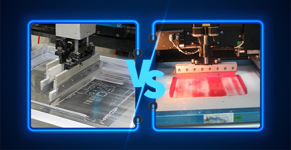
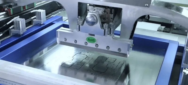
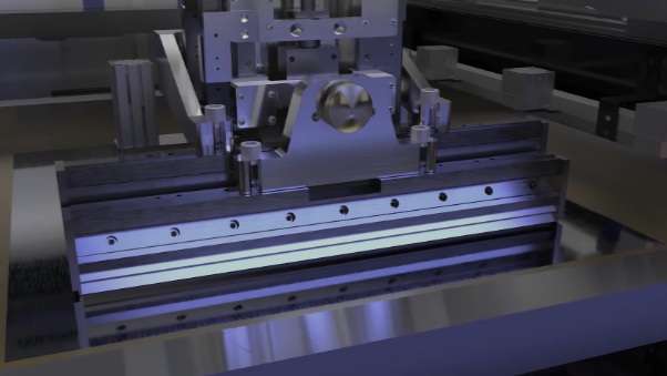
The SMT stencil is aligned over the PCB so that its apertures match the PCB pads exactly. A squeegee spreads solder paste over the stencil, pushing the paste through the apertures and onto the PCB pads below. After the stencil is removed, the solder paste remains precisely on the pads, ready for component placement and subsequent soldering in a reflow oven.
This process ensures that the right amount of solder paste is applied uniformly and consistently, which is critical for producing high-quality solder joints and reliable electronic assemblies.
Types of SMT Stencils
There are several types of SMT stencils designed to meet different manufacturing needs:
- Framed Stencils: These come attached to a metal frame for stability and are ideal for high-volume production due to ease of handling and alignment.
- Frameless Stencils: These are just the stencil sheets without a frame, often used for prototyping or low-volume production.
- Step Stencils: These have varying thicknesses in different areas to control solder paste volume for components of different sizes.
- Electroformed Stencils: Made by electroplating, these offer very fine aperture definition and are used for the most precise applications.
Materials and Thickness
The choice of stencil material affects durability and print quality. Stainless steel is the most common due to its strength and resistance to wear. Nickel stencils offer excellent aperture definition but are more expensive. The thickness of the stencil typically ranges from a few microns to hundreds of microns, depending on the solder paste volume required for the components.

Key Differences Between SMT Stencil and PCB
| Aspect | SMT Stencil | PCB (Printed Circuit Board) |
| Definition | Thin metal sheet with apertures for solder paste application | Laminated board with conductive traces and pads for mounting components |
| Primary Function | Applies solder paste precisely on PCB pads | Provides the physical and electrical platform for electronic components |
| Material | Stainless steel or nickel | Fiberglass, epoxy resin, copper, and other insulating/conductive materials |
| Role in Assembly | Enables accurate solder paste deposition | Houses components and connects them electrically |
| Physical Form | Thin sheet with cutouts | Rigid board with printed circuitry |
| Reusability | Reusable for multiple print cycles | Single-use per assembly |
| Manufacturing Process | Laser-cut or chemically etched apertures | Fabricated through etching, drilling, and layering |
This comparison highlights that SMT stencils and PCBs are complementary tools in SMT assembly rather than interchangeable items.
Why Is the SMT Stencil Important in PCB Assembly?
The SMT stencil is a critical enabler for high-quality SMT assembly. Without it, applying solder paste manually would be inconsistent, slow, and prone to defects such as insufficient solder, bridging, or misalignment.
Benefits of Using SMT Stencils
- Precision: Ensures the exact amount of solder paste is applied to each pad, which is essential for reliable solder joints.
- Consistency: Provides uniform paste application across multiple boards, improving yield and reducing defects.
- Speed: Accelerates the solder paste application process, making it suitable for mass production.
- Cost-Effectiveness: Reduces the need for manual labor and rework, lowering overall manufacturing costs.
- Quality Improvement: Leads to better solder joint quality, which enhances the performance and durability of the final product.
Impact on Assembly Yield and Reliability
The use of SMT stencils directly impacts the yield of PCB assembly. Poor solder paste application can lead to solder bridges (short circuits), tombstoning (components standing up on one end), insufficient solder joints, and other defects. These issues cause rework, scrap, and reliability problems in the field.
By controlling solder paste volume and placement, SMT stencils help maintain consistent solder joint quality, which is critical for high-reliability applications such as aerospace, automotive, and medical devices.
The Relationship Between SMT Stencil and PCB
The SMT stencil is designed specifically for a particular PCB layout. The apertures on the stencil correspond precisely to the solder pads on the PCB. This means that for every PCB design, a matching SMT stencil must be created.
During the assembly process:
1. The PCB is prepared and placed on the stencil printer.
2. The SMT stencil is aligned over the PCB with high precision.
3. Solder paste is applied through the stencil apertures onto the PCB pads.
4. Components are placed on the solder-pasted pads.
5. The assembly is passed through a reflow oven to melt the solder paste and secure the components.
This workflow shows how the SMT stencil and PCB work hand-in-hand to enable efficient and accurate surface mount assembly.
Design Collaboration Between PCB and SMT Stencil
Because the SMT stencil must match the PCB pads exactly, the stencil manufacturer requires detailed PCB design files, especially the solder mask layer and pad layout. Any changes in the PCB design may necessitate a new stencil design.
Designers often optimize PCB pad sizes and shapes to improve stencil printing performance. For example, pad openings and solder mask clearances are adjusted to ensure good solder paste release and minimize defects.
Common Misconceptions About SMT Stencil vs PCB
- SMT stencil is not a PCB: Although sometimes called a PCB stencil, the stencil is only a tool used during the PCB assembly process.
- SMT stencil does not carry components: The stencil only deposits solder paste; it does not hold or connect components.
- PCBs cannot be used without SMT stencils for SMT assembly: While manual soldering is possible, SMT stencils are essential for automated, high-quality SMT production.
- Stencil thickness does not affect solder joint quality: In reality, stencil thickness is a critical parameter that controls the volume of solder paste deposited and thus affects joint reliability.
- One stencil fits all PCBs: Each PCB design requires a custom stencil to match its pad layout exactly.
Advanced Considerations in SMT Stencil and PCB Interaction
Fine Pitch Components and Stencil Design
With the trend toward miniaturization, components such as BGAs (Ball Grid Arrays), QFNs (Quad Flat No-leads), and CSPs (Chip Scale Packages) have very fine pitch pads. Designing SMT stencils for these components requires extremely precise aperture shapes and sizes to avoid solder bridging and insufficient solder.
Specialized stencil technologies such as electroformed stencils and laser-cut step stencils are often used to handle these challenges.
Solder Paste Types and Stencil Compatibility
Different solder pastes have varying viscosities and particle sizes, which can influence stencil design choices. For example, ultra-fine solder particles require finer apertures and more precise stencil manufacturing to ensure proper paste release.
Cleaning and Maintenance of SMT Stencils
SMT stencils must be cleaned regularly to remove solder paste residues and prevent clogging of apertures. Proper cleaning extends stencil life and maintains print quality. Automated stencil cleaning machines are commonly used in production environments.
Conclusion
Understanding the difference between SMT stencil and PCB is fundamental for electronics manufacturing. The PCB serves as the physical and electrical foundation of electronic devices, while the SMT stencil is a precision tool used to apply solder paste accurately onto the PCB during assembly. Together, they enable the efficient, reliable, and high-quality production of modern electronic products. The SMT stencil ensures that solder paste is deposited consistently and precisely, which directly impacts the quality of solder joints and the overall performance of the assembled PCB. Without either of these, modern electronics manufacturing would be far less efficient and far more error-prone.
The synergy between SMT stencil and PCB design is a cornerstone of surface mount technology, enabling the mass production of compact, complex, and reliable electronic devices that power today's digital world.

FAQ
1. What is the main function of an SMT stencil in PCB assembly?
The main function of an SMT stencil is to apply solder paste precisely onto the PCB pads where surface-mount components will be placed. It ensures accurate and consistent solder paste deposition for reliable solder joints.
2. Can a PCB be assembled without using an SMT stencil?
While it is technically possible to assemble a PCB without an SMT stencil by manually applying solder paste, it is highly inefficient and prone to errors. SMT stencils are critical for automated, high-volume, and high-quality SMT assembly.
3. What materials are SMT stencils typically made from?
SMT stencils are usually made from stainless steel or nickel. These materials offer the precision, durability, and fine aperture definition required for accurate solder paste application.
4. How does the SMT stencil relate to the PCB design?
The SMT stencil is custom-made to match the PCB design. The apertures on the stencil correspond exactly to the solder pads on the PCB to ensure precise solder paste application.
5. What are the different types of SMT stencils?
The main types of SMT stencils include framed stencils, frameless stencils, step stencils, and electroformed stencils. Each type serves different production needs, from high-volume manufacturing to prototyping and handling components of varying sizes.


