Content Menu
● Introduction
● What is Surface Mounting Technology?
>> Key Components of SMT
● Advantages of Surface Mounting Technology
>> 1. Miniaturization
>> 2. Increased Production Efficiency
>> 3. Improved Performance
>> 4. Cost-Effectiveness
>> 5. Flexibility in Design
● Challenges of Surface Mounting Technology
>> 1. Handling and Placement
>> 2. Thermal Management
>> 3. Repair and Rework
>> 4. Design Complexity
● The SMT Process
>> 1. Design and Layout
>> 2. Solder Paste Application
>> 3. Component Placement
>> 4. Reflow Soldering
>> 5. Inspection and Testing
● Applications of Surface Mounting Technology
● Conclusion
● Related Questions
>> 1. What is the difference between SMT and through-hole technology?
>> 2. What are the main advantages of using SMT?
>> 3. What challenges does SMT present?
>> 4. How does the SMT process work?
>> 5. In what industries is SMT commonly used?
Introduction
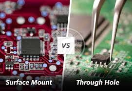
Surface Mounting Technology (SMT) is a revolutionary method in the electronics manufacturing industry that has transformed how electronic components are assembled onto printed circuit boards (PCBs). This technique allows for the direct mounting of components on the surface of PCBs, which contrasts with traditional through-hole technology where components are inserted into drilled holes. The adoption of SMT has led to significant advancements in the miniaturization of electronic devices, increased production efficiency, and improved performance. In this article, we will delve into the intricacies of SMT, its advantages, challenges, and its impact on modern electronics.

What is Surface Mounting Technology?
Surface Mounting Technology refers to a method of assembling electronic components directly onto the surface of a PCB. This process involves the use of surface mount devices (SMDs), which are components designed specifically for this type of assembly. SMDs are typically smaller and lighter than their through-hole counterparts, allowing for more compact designs and higher component density on PCBs.
Key Components of SMT
1. Surface Mount Devices (SMDs): These are the electronic components that are mounted directly onto the PCB surface. They can include resistors, capacitors, integrated circuits, and more.
2. Printed Circuit Boards (PCBs): The substrate on which SMDs are mounted. PCBs are designed with specific layouts to accommodate various components.
3. Solder Paste: A mixture of solder and flux that is applied to the PCB pads where SMDs will be placed. It helps in creating a strong electrical connection when heated.
4. Reflow Oven: A specialized oven used to heat the solder paste, causing it to melt and form a solid connection between the SMDs and the PCB.
Advantages of Surface Mounting Technology
1. Miniaturization
One of the most significant benefits of SMT is the ability to create smaller and lighter electronic devices. As consumer demand for compact gadgets increases, SMT allows manufacturers to design products that occupy less space without compromising functionality.
2. Increased Production Efficiency
SMT enables faster assembly processes. Automated pick-and-place machines can quickly position SMDs on PCBs, significantly reducing assembly time compared to manual processes. This efficiency translates to lower production costs and faster time-to-market for new products.
3. Improved Performance
The shorter electrical paths in SMT designs can lead to better performance in terms of signal integrity and reduced electromagnetic interference. This is particularly important in high-frequency applications where performance is critical.
4. Cost-Effectiveness
While the initial setup for SMT may be higher due to the need for specialized equipment, the overall cost savings in production and materials often outweigh these initial investments. The ability to use smaller components also reduces material costs.
5. Flexibility in Design
SMT allows for more complex circuit designs. Engineers can incorporate a greater variety of components in a smaller area, enabling innovative product designs that were previously impossible with through-hole technology.

Challenges of Surface Mounting Technology
Despite its many advantages, SMT also presents several challenges that manufacturers must navigate.
1. Handling and Placement
SMDs are often smaller and more delicate than through-hole components, making them more challenging to handle and place accurately. This requires precise machinery and careful handling to avoid damage.
2. Thermal Management
The compact nature of SMT can lead to issues with heat dissipation. As more components are packed into a smaller space, managing heat becomes critical to ensure reliability and performance.
3. Repair and Rework
Repairing or replacing SMDs can be more complicated than through-hole components. Specialized tools and techniques are often required to desolder and resolder components without damaging the PCB.
4. Design Complexity
While SMT allows for more complex designs, it also requires more sophisticated design tools and expertise. Engineers must be well-versed in SMT principles to create effective layouts.
The SMT Process
The SMT process involves several key steps:
1. Design and Layout
The first step is designing the PCB layout, which includes determining the placement of SMDs and the routing of electrical connections. This design must consider factors such as component size, spacing, and thermal management.
2. Solder Paste Application
Solder paste is applied to the PCB pads using a stencil or screen printing method. This paste will later be melted to create the electrical connections.
3. Component Placement
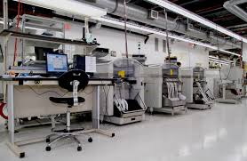
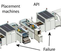
Automated pick-and-place machines position the SMDs onto the solder paste-covered pads. This step requires high precision to ensure that components are correctly aligned.
4. Reflow Soldering
The PCB is passed through a reflow oven, where the solder paste is heated to its melting point. This process creates a solid electrical connection between the SMDs and the PCB.
5. Inspection and Testing
After soldering, the assembled PCBs undergo inspection and testing to ensure that all components are correctly placed and functioning as intended. This may involve visual inspection, automated optical inspection (AOI), and functional testing.
Applications of Surface Mounting Technology
SMT is widely used across various industries, including:
- Consumer Electronics: Smartphones, tablets, and laptops utilize SMT for their compact designs.
- Automotive: Modern vehicles incorporate numerous electronic systems that rely on SMT for reliability and performance.
- Medical Devices: SMT is crucial in the development of compact and efficient medical equipment.
- Telecommunications: High-frequency devices benefit from the performance advantages of SMT.
Conclusion
Surface Mounting Technology has fundamentally changed the landscape of electronics manufacturing. Its ability to facilitate miniaturization, improve production efficiency, and enhance performance makes it an essential technique in modern electronics. While challenges exist, the benefits of SMT far outweigh the drawbacks, making it the preferred choice for many manufacturers. As technology continues to evolve, SMT will undoubtedly play a pivotal role in shaping the future of electronic devices.

Related Questions
1. What is the difference between SMT and through-hole technology?
SMT involves mounting components directly on the surface of a PCB, while through-hole technology requires components to be inserted into drilled holes. SMT allows for smaller, more compact designs.
2. What are the main advantages of using SMT?
The main advantages include miniaturization, increased production efficiency, improved performance, cost-effectiveness, and design flexibility.
3. What challenges does SMT present?
Challenges include handling and placement of small components, thermal management, repair and rework difficulties, and increased design complexity.
4. How does the SMT process work?
The SMT process involves designing the PCB layout, applying solder paste, placing components, reflow soldering, and inspecting the final product.
5. In what industries is SMT commonly used?
SMT is commonly used in consumer electronics, automotive, medical devices, and telecommunications.


