Content Menu
● Understanding SMT PCB Spacers
● Key Innovations Driving SMT PCB Spacer Development
>> 1. Integration with Automated SMT Assembly Lines
>> 2. Enhanced Material and Design Engineering
>> 3. Diverse Spacer Configurations for Specialized Applications
>> 4. Process Reliability and Cost Efficiency
>> 5. Environmental and Regulatory Compliance
● Additional Innovations Enhancing SMT PCB Spacer Performance
>> 6. Thermal Management Capabilities
>> 7. Miniaturization and High-Density Packaging
>> 8. Smart Spacer Technologies
● Benefits of SMT PCB Spacers in Modern Electronics
● Conclusion
● FAQ About SMT PCB Spacers
>> 1. What are SMT PCB spacers used for?
>> 2. How do SMT PCB spacers improve the assembly process?
>> 3. What materials are SMT PCB spacers made from?
>> 4. Can SMT PCB spacers be customized?
>> 5. Are SMT PCB spacers environmentally compliant?
Surface Mount Technology (SMT) has become a cornerstone in modern electronics manufacturing, enabling compact, efficient, and highly reliable printed circuit board (PCB) assemblies. Among the many components that benefit from SMT advancements, SMT PCB spacers have emerged as critical enablers for improved assembly processes and device performance. This article explores the latest innovations driving the development of SMT PCB spacers, their benefits, and how they are transforming electronic manufacturing.

Understanding SMT PCB Spacers
SMT PCB spacers are specialized components used to maintain precise distances between PCBs or between a PCB and other parts of an electronic assembly. Unlike traditional spacers that require manual insertion and fastening, SMT PCB spacers are designed to be mounted directly onto the PCB surface using surface mount technology. This allows them to be placed automatically alongside other SMT components during the reflow soldering process.
These spacers provide mechanical support, ensure electrical isolation, and help achieve optimal board-to-board spacing, which is essential for heat dissipation, component clearance, and overall device reliability. Their role is especially critical in multi-layer or multi-board assemblies where precise spacing affects not only mechanical stability but also signal integrity and thermal management.
Key Innovations Driving SMT PCB Spacer Development
1. Integration with Automated SMT Assembly Lines
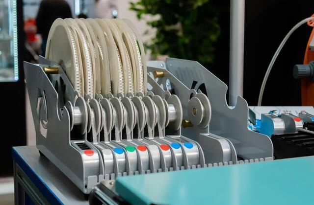
One of the most significant innovations in SMT PCB spacers is their compatibility with automated SMT assembly equipment. For example, PENCOM's TDU Surface-Mount Spacers are packaged on tape and reel, enabling seamless pick-and-place installation alongside other SMT components. This integration dramatically reduces manual handling, accelerates assembly times, and minimizes the risk of PCB damage during production.
Automated placement also ensures precise spacer positioning, which is critical for maintaining consistent board-to-board heights and mechanical stability. This shift from manual to automated placement aligns with the broader electronics manufacturing trend toward Industry 4.0, where automation and data exchange drive efficiency and quality.
2. Enhanced Material and Design Engineering
Modern SMT PCB spacers are engineered from advanced materials that withstand multiple reflow soldering cycles without degradation. Würth Elektronik's SMT spacers, for instance, feature specially developed plating that prevents discoloration, cracking, or blistering during soldering. This durability allows for robust mechanical connections and reliable electrical isolation.
Moreover, innovations in spacer geometry and solder pad design optimize solder wetting and holding forces, ensuring strong attachment to the PCB and enabling the use of threaded or through-hole variants for versatile mounting options. Some spacers incorporate high-temperature resistant polymers or plated metals that maintain mechanical integrity in harsh operating environments.
3. Diverse Spacer Configurations for Specialized Applications
SMT PCB spacers now come in a wide array of sizes, shapes, and orientations to meet diverse application needs. Available heights range from as low as 0.5mm to 16mm, with options for vertical or right-angle mounting. This flexibility allows designers to tailor board spacing for complex multi-board assemblies, housing integration, or thermal management requirements.
Specialized versions such as reverse spacers enable connections to the bottom side of single-sided PCBs, eliminating the need for additional soldering steps and simplifying assembly. Additionally, some spacers are designed with built-in threading or captive nuts, facilitating easy mechanical fastening and disassembly for maintenance or upgrades.
4. Process Reliability and Cost Efficiency
By enabling fully automated assembly, SMT PCB spacers reduce manual labor, lower scrap rates, and enhance process repeatability. The streamlined installation process cuts down on PCB handling and potential damage, improving overall yield and reducing production costs.
The ability to order custom spacer lengths and configurations further optimizes inventory management and procurement, contributing to cost savings and supply chain efficiency. Furthermore, the reduction in assembly time and labor costs can significantly impact the total cost of ownership, especially in high-volume manufacturing environments.
5. Environmental and Regulatory Compliance
As SMT technology evolves, environmental considerations have become integral to spacer development. Manufacturers are adopting lead-free solder compatibility and RoHS-compliant materials for SMT PCB spacers to meet global regulatory standards. This ensures that electronic assemblies incorporating these spacers align with sustainability goals and market requirements.
Additionally, some manufacturers are exploring recyclable materials and eco-friendly plating processes to reduce the environmental footprint of their components. This focus on sustainability is increasingly important as electronics manufacturers face stricter regulations and consumer demand for greener products.

Additional Innovations Enhancing SMT PCB Spacer Performance
6. Thermal Management Capabilities
With the increasing power density of modern electronic devices, thermal management has become a critical design consideration. Some SMT PCB spacers are now being developed with thermally conductive materials or coatings that facilitate heat dissipation between stacked boards. This innovation helps prevent overheating and improves the reliability and lifespan of electronic assemblies.
Thermally enhanced spacers can also serve as heat paths, transferring heat away from sensitive components to heat sinks or chassis, thereby integrating mechanical support with thermal management in a single component.
7. Miniaturization and High-Density Packaging
As consumer electronics and IoT devices shrink in size, the demand for smaller and more compact components increases. Innovations in SMT PCB spacer miniaturization allow for ultra-low profile spacers that occupy minimal board space while maintaining mechanical strength. These tiny spacers enable high-density packaging and multi-layer PCB stacks without compromising assembly reliability.
Advanced manufacturing techniques such as micro-machining and precision molding contribute to producing these miniature spacers with tight tolerances and consistent quality.
8. Smart Spacer Technologies
Emerging trends include integrating sensors or conductive pathways within SMT PCB spacers to enable smart functionalities. For instance, spacers equipped with embedded temperature or strain sensors can provide real-time monitoring of mechanical stress or thermal conditions within the PCB stack.
Such smart spacers can feed data to system controllers, allowing predictive maintenance, improved fault detection, and enhanced device reliability. While still in early stages, this innovation points towards a future where passive components like spacers contribute actively to system intelligence.
Benefits of SMT PCB Spacers in Modern Electronics
- Compact and High-Density Assemblies: SMT spacers support the trend toward miniaturization by enabling precise board-to-board spacing without bulky hardware.
- Improved Mechanical Stability: They provide reliable fixation for PCBs and components, reducing mechanical stress and vibration effects in devices.
- Faster Production Times: Automated placement and soldering accelerate assembly lines and improve throughput.
- Cost Reduction: Less manual labor and fewer defects translate into lower manufacturing costs.
- Design Flexibility: Wide variety of spacer types and sizes allow engineers to optimize layouts for performance and manufacturability.
- Enhanced Thermal Management: Thermally conductive spacers help dissipate heat in high-power applications.
- Environmental Compliance: Lead-free and RoHS-compliant materials support sustainable manufacturing.
Conclusion
The development of SMT PCB spacers is driven by innovations that enhance automation compatibility, material robustness, design versatility, process reliability, and environmental compliance. These advancements are transforming how electronic assemblies are built, enabling faster production, higher quality, and more compact designs.
From integration with automated SMT lines to the use of advanced materials and the emergence of smart spacer technologies, the evolution of SMT PCB spacers reflects the broader trends in electronics manufacturing toward efficiency, miniaturization, and sustainability. As SMT technology continues to evolve, SMT PCB spacers will play an increasingly vital role in meeting the demands of next-generation electronic devices, ensuring mechanical stability, thermal management, and assembly precision.

FAQ About SMT PCB Spacers
1. What are SMT PCB spacers used for?
SMT PCB spacers are used to maintain precise spacing between PCBs or between a PCB and other components, providing mechanical support, electrical isolation, and ensuring proper clearance for thermal and functional requirements.
2. How do SMT PCB spacers improve the assembly process?
They enable fully automated placement alongside other SMT components, reducing manual labor, minimizing PCB handling damage, and accelerating assembly line throughput.
3. What materials are SMT PCB spacers made from?
They are typically made from durable materials with special plating that withstand multiple reflow soldering cycles without discoloration or cracking, ensuring long-term reliability.
4. Can SMT PCB spacers be customized?
Yes, many manufacturers offer custom lengths, hole diameters, and configurations to meet specific project requirements, enhancing design flexibility and inventory efficiency.
5. Are SMT PCB spacers environmentally compliant?
Modern SMT PCB spacers are designed to be compatible with lead-free solder and meet RoHS standards, supporting environmentally sustainable electronics manufacturing.


