Content Menu
● Introduction to Surface Mount Technology
● Key Steps in the Surface Mount Technology Process Flow
>> Material Preparation
>> Stencil Preparation
>> Solder Paste Printing
>> Component Placement
>> Reflow Soldering
>> Inspection
>> Final Cleaning and Testing
● Advantages of Surface Mount Technology
● Conclusion
● Related Questions
>> 1. What is the difference between SMT and through-hole technology?
>> 2. How does solder paste affect the SMT process?
>> 3. What types of components are used in SMT?
>> 4. What are common defects in the SMT process?
>> 5.How can quality control be improved in SMT?
Surface Mount Technology (SMT) has transformed the electronics manufacturing landscape by enabling the efficient assembly of electronic components onto printed circuit boards (PCBs). This article delves into the key steps involved in the SMT process flow, highlighting its significance, advantages, and the intricate details that ensure high-quality electronic products.

Introduction to Surface Mount Technology
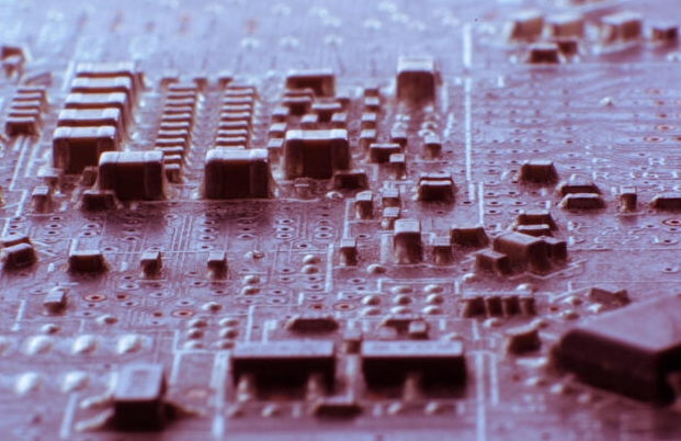
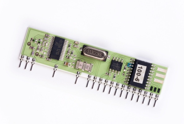
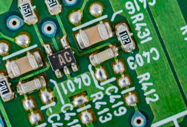
Surface Mount Technology is a method that allows electronic components to be mounted directly onto the surface of PCBs. Unlike traditional through-hole technology, where components are inserted into holes in the PCB, SMT components are soldered onto pads on the board's surface. This technique offers several advantages, including reduced space requirements, improved performance, and the ability to automate the assembly process.
Key Steps in the Surface Mount Technology Process Flow
The SMT process flow consists of several critical steps, each contributing to the overall efficiency and effectiveness of the assembly process. Below are the key steps involved:
Material Preparation
Before the SMT process begins, it is essential to prepare the materials. This includes selecting the appropriate surface mount components (SMCs) and ensuring that the PCBs are designed to accommodate these components. The design phase involves creating a layout that specifies the placement of components, pad sizes, and routing for electrical connections.
Stencil Preparation
Once the materials are ready, the next step is stencil preparation. A stencil is used to apply solder paste to the PCB pads where the components will be placed. The stencil is typically made of stainless steel or a similar material and is designed to match the layout of the PCB. Proper stencil preparation is crucial for ensuring that the right amount of solder paste is applied, which directly affects the quality of the solder joints.
Solder Paste Printing
After preparing the stencil, the solder paste is printed onto the PCB. This step involves aligning the stencil with the PCB and using a squeegee to spread the solder paste over the stencil openings. The goal is to deposit a precise amount of solder paste on each pad, which will later facilitate the soldering of the components.
Component Placement
With the solder paste applied, the next step is component placement. Automated pick-and-place machines are commonly used in this stage to accurately position the SMCs onto the solder paste-covered pads. These machines utilize vision systems to ensure precise placement, which is critical for maintaining the integrity of the solder joints.

Reflow Soldering
Once the components are placed, the PCB moves to the reflow soldering stage. This process involves heating the PCB in a reflow oven, where the solder paste melts and forms a solid connection between the components and the PCB pads. The reflow process is carefully controlled to ensure that the solder reaches the appropriate temperature for a sufficient amount of time, allowing for proper wetting and bonding.
Inspection
After reflow soldering, the assembled PCB undergoes inspection to ensure that all components are correctly placed and soldered. Automated optical inspection (AOI) systems are often employed to detect any defects, such as misaligned components or insufficient solder joints. This step is crucial for maintaining high-quality standards in electronic manufacturing.
Final Cleaning and Testing
The final steps in the SMT process flow involve cleaning the PCB to remove any flux residues and conducting functional tests to verify that the assembled board operates as intended. Cleaning can be done using various methods, including ultrasonic cleaning or using solvents. Functional testing ensures that the electronic device meets its specifications and is ready for deployment.
Advantages of Surface Mount Technology
The adoption of Surface Mount Technology offers numerous benefits, including:
- Space Efficiency: SMT components are generally smaller than their through-hole counterparts, allowing for more compact PCB designs.
- Increased Performance: The shorter electrical paths in SMT can lead to improved signal integrity and reduced electromagnetic interference.
- Automation: The SMT process is highly amenable to automation, which can significantly reduce labor costs and increase production speed.
- Flexibility: SMT allows for a wide variety of components to be used, including passive and active devices, which can be placed on both sides of the PCB.
Conclusion
In conclusion, the Surface Mount Technology process flow is a complex yet highly efficient method for assembling electronic components onto PCBs. Each step, from material preparation to final inspection, plays a vital role in ensuring the quality and reliability of electronic devices. As technology continues to advance, SMT will remain a cornerstone of modern electronics manufacturing, enabling the production of smaller, faster, and more efficient devices.

Related Questions
1. What is the difference between SMT and through-hole technology?
The primary difference lies in the mounting method; SMT components are soldered directly onto the surface of the PCB, while through-hole components are inserted into holes and soldered from the opposite side.
2. How does solder paste affect the SMT process?
Solder paste is crucial for creating reliable solder joints. The amount and quality of solder paste applied directly influence the strength and integrity of the connections between components and the PCB.
3. What types of components are used in SMT?
SMT can accommodate a wide range of components, including resistors, capacitors, integrated circuits, and connectors, all designed for surface mounting.
4. What are common defects in the SMT process?
Common defects include misalignment of components, insufficient solder, solder bridging, and component tombstoning, where one end of a component lifts off the PCB.
5.How can quality control be improved in SMT?
Quality control can be enhanced through regular inspection using AOI systems, implementing strict process controls, and conducting thorough testing of assembled boards.


