Content Menu
● Understanding SMT Stencils and Their Role in PCB Production
>> The Importance of SMT Stencils in High-Volume PCB Assembly
● Types of SMT Stencils
>> Laser-Cut Stencils
>> Electroformed Stencils
>> Framed vs. Frameless Stencils
>> Step Stencils
● SMT Stencil Production Processes
>> Laser Cutting
>> Chemical Etching
>> Electroforming
● Best Practices for Using SMT Stencils in High-Volume PCB Production
>> 1. Accurate PCB and Stencil Alignment
>> 2. Optimal Solder Paste Application
>> 3. Secure PCB Mounting
>> 4. Choose Appropriate Stencil Thickness
>> 5. Regular Stencil Cleaning and Inspection
● Optimizing SMT Stencils for High-Volume Production
>> Aperture Design and Size Optimization
>> Material Selection
>> Integration with Automated Printing Equipment
● Challenges and Solutions in SMT Stencil Usage for High-Volume PCB Production
● Conclusion
● FAQ
>> 1. What materials are commonly used for SMT stencils?
>> 2. How does stencil thickness affect solder paste printing?
>> 3. Why is stencil alignment important in SMT printing?
>> 4. How often should SMT stencils be cleaned?
>> 5. What are the main advantages of laser-cut SMT stencils?
Surface Mount Technology (SMT) stencils are indispensable tools in the high-volume manufacturing of printed circuit boards (PCBs). They play a crucial role in ensuring precise and consistent solder paste deposition, which directly impacts the quality, reliability, and yield of PCB assemblies. In this comprehensive article, we will explore how to effectively use SMT stencils in large-scale PCB production. We will cover everything from stencil types and manufacturing processes to best practices, optimization techniques, and common challenges faced during SMT stencil usage.

Understanding SMT Stencils and Their Role in PCB Production
An SMT stencil is a thin, flat sheet—usually made from stainless steel or nickel—with carefully designed apertures that correspond exactly to the solder pads on a PCB. During the assembly process, solder paste is applied through these apertures onto the PCB pads, allowing surface mount devices (SMDs) to be soldered accurately and efficiently.
The Importance of SMT Stencils in High-Volume PCB Assembly
In high-volume PCB manufacturing, the use of SMT stencils is critical for several reasons:
- Precision: SMT stencils control the exact volume and placement of solder paste, which is essential to avoid defects such as solder bridging (where solder connects two adjacent pads unintentionally) or insufficient solder joints that can cause component failure.
- Speed: Automated stencil printing drastically reduces the time required to apply solder paste compared to manual methods, enabling manufacturers to meet demanding production schedules.
- Repeatability: High-volume production demands consistent solder paste deposition across thousands or even millions of PCBs. Stencils provide the repeatability needed to maintain quality and reduce costly rework or scrap rates.
Types of SMT Stencils
Selecting the right type of SMT stencil is fundamental to achieving optimal results in PCB assembly. The choice depends on the PCB design complexity, component types, production volume, and budget.
| Stencil Type | Description | Advantages |
| Laser-Cut Stencils | Made from thin stainless steel sheets with laser-cut apertures matching PCB pads. | High precision, suitable for complex designs, durable, reusable. |
| Electroformed Stencils | Created via electroforming to produce very fine and accurate apertures. | Superior accuracy, excellent for fine-pitch components, highly durable. |
| Framed Stencils | Stencils mounted on a frame for stability during printing. | Better support for large PCBs, easier alignment. |
| Frameless Stencils | Stencils without frames, lighter and more flexible. | Suitable for smaller or less complex PCBs. |
| Step Stencils | Stencils with varying thicknesses in different areas to control solder volume. | Optimizes solder paste volume for mixed component sizes. |
Laser-Cut Stencils
Laser-cut stencils are the most common type used in PCB assembly. The laser cutting process produces apertures with tapered walls, which helps in the smooth release of solder paste onto the PCB pads. These stencils offer excellent precision and durability, making them suitable for a wide range of PCB designs, including those with fine-pitch components.
Electroformed Stencils
Electroformed stencils are manufactured through an electroplating process that deposits metal onto a patterned mandrel. This method produces extremely precise apertures with very smooth edges, ideal for ultra-fine-pitch components and high-density PCB layouts. Although electroformed stencils are more expensive, their superior accuracy and longevity often justify the cost for high-volume, high-precision production.
Framed vs. Frameless Stencils
Framed stencils are mounted on rigid frames, which provide stability during the printing process and simplify handling, especially for large PCBs. Frameless stencils, on the other hand, are simply the metal sheet without a frame, making them lighter and more flexible. Frameless stencils are often used for smaller PCBs or low-volume production where ease of handling is less critical.
Step Stencils
Step stencils have areas of different thicknesses, allowing manufacturers to deposit varying amounts of solder paste on different parts of the PCB. This is particularly useful when a PCB contains both fine-pitch components that require minimal solder paste and larger components that need more solder volume for reliable joints.
SMT Stencil Production Processes
The quality of SMT stencils significantly influences the solder paste printing process and, consequently, the overall PCB assembly quality. Understanding the common stencil manufacturing methods helps in selecting the right stencil for your production needs.
Laser Cutting
Laser cutting is the most widely used method for producing SMT stencils. A high-powered laser beam precisely cuts the apertures into thin stainless steel sheets according to the PCB pad layout. This process allows for rapid production of stencils with complex aperture shapes and sizes. The laser-cut apertures typically have a tapered wall profile, which improves solder paste release and reduces the risk of clogging.
Chemical Etching
Chemical etching is a traditional method where the stencil sheet is coated with a photoresist, exposed to UV light through a mask, and then etched with acid to create apertures. While this method is less expensive, it offers lower precision and less control over aperture tapering compared to laser cutting, making it less suitable for fine-pitch or high-density PCB designs.
Electroforming
Electroforming involves depositing metal onto a patterned mandrel to create a stencil with extremely precise and smooth apertures. This process produces stencils with the highest accuracy and durability, ideal for advanced PCBs with very fine-pitch components. Electroformed stencils are often used in high-volume production runs where reliability and repeatability are paramount.

Best Practices for Using SMT Stencils in High-Volume PCB Production
To maximize the benefits of SMT stencils in high-volume PCB assembly, manufacturers should follow these best practices:
1. Accurate PCB and Stencil Alignment
Proper alignment between the stencil and PCB is essential to ensure solder paste is deposited exactly on the pads. Automated stencil printers use optical sensors to detect fiducial marks on both the PCB and stencil, enabling precise registration. Misalignment can cause solder paste to miss pads or bridge adjacent pads, leading to assembly defects.
2. Optimal Solder Paste Application
The solder paste application process must be carefully controlled to ensure consistent deposition:
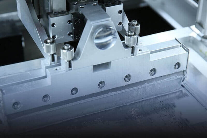
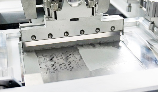
- Use a squeegee blade at a 15-20 degree angle to spread solder paste evenly across the stencil surface.
- Maintain consistent, moderate pressure on the squeegee to fill stencil apertures without damaging the stencil or PCB.
- Control the speed of the squeegee to balance paste volume and print quality.
3. Secure PCB Mounting
The PCB must be firmly fixed during printing to prevent movement that can cause misalignment or smearing of solder paste. Mechanical clamps, vacuum fixtures, or support pins can be used to stabilize the PCB and maintain flatness.
4. Choose Appropriate Stencil Thickness
Stencil thickness directly affects the volume of solder paste deposited:
- Thicker stencils (100-150 microns) are suitable for larger components that require more solder.
- Thinner stencils (50-75 microns) are ideal for fine-pitch components where excess solder can cause bridging.
Selecting the right thickness helps prevent solder defects and ensures reliable solder joints.
5. Regular Stencil Cleaning and Inspection
Solder paste residue can clog stencil apertures, leading to inconsistent printing and defects. Stencils should be cleaned frequently during production runs using appropriate solvents or automated cleaning systems. Additionally, regular inspection of stencil apertures for wear, deformation, or damage ensures consistent print quality and prolongs stencil life.
Optimizing SMT Stencils for High-Volume Production
Aperture Design and Size Optimization
The design and size of stencil apertures are critical factors in solder paste printing quality. Apertures must match the size and shape of PCB pads and component leads to ensure proper solder joint formation. Oversized apertures can cause solder bridging, while undersized apertures may result in insufficient solder.
Advanced aperture shapes such as trapezoidal or rounded apertures can improve solder paste release and reduce defects. Additionally, adjusting aperture size allows manufacturers to control solder paste volume precisely, optimizing the solder joint for each component type.
Material Selection
Material choice affects stencil durability and print quality:
- Stainless Steel: The most common material, offering good durability, corrosion resistance, and consistent print quality.
- Nickel Electroformed: Provides superior precision and longer lifespan, especially beneficial for fine-pitch and high-density PCBs.
Choosing the right material based on production volume and PCB complexity helps balance cost and performance.
Integration with Automated Printing Equipment
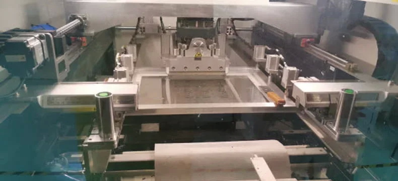
Automated stencil printers equipped with conveyor systems and optical alignment features maximize throughput and repeatability in high-volume production. Automation reduces human error, ensures consistent solder paste deposition, and enables faster changeovers between PCB batches.
Challenges and Solutions in SMT Stencil Usage for High-Volume PCB Production
| Challenge | Solution |
| Solder paste smearing or bridging | Optimize aperture size and stencil thickness; maintain proper squeegee pressure and angle. |
| Stencil clogging | Implement frequent cleaning cycles and use high-quality solder paste with appropriate viscosity. |
| Misalignment | Employ automated optical alignment and fiducial mark registration to ensure precision. |
| Wear and tear of stencil | Use durable materials like electroformed nickel and schedule regular stencil replacement to maintain print quality. |
| Variability in solder paste volume | Use step stencils or adjust aperture design to control solder volume for mixed component sizes. |
Addressing these challenges proactively helps maintain consistent solder paste printing quality and reduces defects in high-volume PCB production.
Conclusion
Effectively using SMT stencils is pivotal for achieving high-quality, high-volume PCB assembly. The stencil is the foundation for precise solder paste deposition, which directly influences solder joint reliability and overall product performance. By selecting the appropriate stencil type and material, optimizing aperture design and stencil thickness, ensuring precise alignment, and integrating automated printing systems, manufacturers can significantly improve solder paste printing accuracy and consistency.
Regular stencil maintenance, including cleaning and inspection, further ensures repeatability and reduces downtime. Overcoming common challenges such as stencil clogging, misalignment, and wear is essential to maintaining high yields and minimizing production costs.
In summary, mastering the use of SMT stencils in high-volume PCB production enables manufacturers to deliver reliable, defect-free assemblies at scale, meeting the demands of modern electronics manufacturing with efficiency and quality.

FAQ
1. What materials are commonly used for SMT stencils?
SMT stencils are primarily made from stainless steel and nickel. Stainless steel is widely used for its durability and print quality, while nickel electroformed stencils offer higher precision and longer lifespan.
2. How does stencil thickness affect solder paste printing?
Stencil thickness determines the volume of solder paste deposited. Thicker stencils deposit more paste, suitable for larger components, whereas thinner stencils are ideal for fine-pitch components requiring less solder.
3. Why is stencil alignment important in SMT printing?
Proper alignment ensures solder paste is deposited exactly on PCB pads, preventing defects such as solder bridging or insufficient solder joints. Automated printers use optical sensors to achieve high precision.
4. How often should SMT stencils be cleaned?
Stencils should be cleaned frequently during production to prevent solder paste clogging apertures, which can cause inconsistent printing and defects.
5. What are the main advantages of laser-cut SMT stencils?
Laser-cut stencils offer high precision, fast production, the ability to create conical apertures for better paste release, and durability suitable for complex PCB designs.


