Content Menu
● Introduction to PCB Test Points
>> Probe Test Points
>> Automated Test Points
● Importance of Test Points in Compact SMT PCBs
● Types of Test Points for Compact SMT PCBs
>> Surface Mount (SMT) Test Points
>> Through-Hole Mounted (THM) Test Points
● Guidelines for Choosing and Placing Test Points
>> Size and Shape
>> Placement
>> Spacing
>> Material and Construction
● Design Considerations for Compact SMT PCBs
>> High-Speed Design
>> Component Placement
>> Tooling Holes
● Advanced Testing Techniques
>> In-Circuit Testing (ICT)
>> Flying Probe Testing (FPT)
● Challenges in Test Point Design
● Conclusion
● FAQs
>> 1. What is the ideal size for a test point on a compact SMT PCB?
>> 2. How should test points be distributed on a compact SMT PCB?
>> 3. What is the minimum spacing recommended between test points?
>> 4. What materials are commonly used for SMT test points?
>> 5. Why is it important to keep test points away from the edge of the PCB?
● Citations:
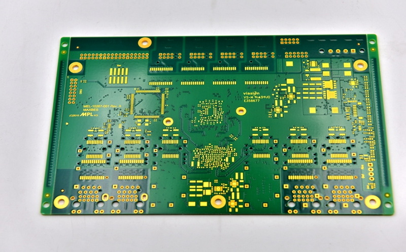
Choosing the right test points for compact Surface Mount Technology (SMT) Printed Circuit Boards (PCBs) is crucial for efficient testing and debugging. Test points are exposed metal pads on the exterior layer of a PCB, allowing probes to contact them for testing purposes. In this article, we will explore the importance of test points, types of test points, and guidelines for selecting and placing them on compact SMT PCBs.

Introduction to PCB Test Points
PCB test points are essential for verifying the functionality of circuits and troubleshooting issues. They enable the injection of test signals to detect potential problems and ensure that the circuit operates as specified. Test points can be categorized into two main types: probe test points for manual testing and automated test points for use with automated test equipment.
Probe Test Points
Probe test points are designed for manual testing using handheld devices or probes. They are typically larger and easily accessible, often marked with reference designators (e.g., "GND" or "PWR") and net names. These points are ideal for surface-level testing to verify proper current supply and ground values. The use of J-hooks or sharp-pointed probes is common for these test points, especially in older PCB styles with leads[1].
Automated Test Points
Automated test points are smaller and used with automated test equipment. They can be vias, through-hole pins, or small metal pads designed to accommodate the probes of automated test systems. Automated testing includes methods like Bare Board Testing (BBT), In-Circuit Testing (ICT), and Flying Probe Testing (FPT). These methods require precise placement and sizing of test points to ensure reliable contact with the test probes[4].
Importance of Test Points in Compact SMT PCBs
In compact SMT PCBs, test points play a vital role due to the high component density and complexity. They help in:
- Debugging and Troubleshooting: Test points allow for quick identification and isolation of faults, reducing repair time and costs.
- Quality Assurance: By ensuring all components are functioning correctly, test points contribute to higher product reliability.
- Design Verification: Test points help verify that the PCB design meets specifications and functions as intended.
Types of Test Points for Compact SMT PCBs
Surface Mount (SMT) Test Points
SMT test points are compact and soldered directly to the PCB, allowing for efficient board-level testing. They are ideal for dense circuit boards and are compatible with automated pick-and-place assembly systems. Keystone Electronics offers a variety of SMT test points, including micro-miniature and hybrid mount types, with silver-plated phosphor bronze terminals.
Through-Hole Mounted (THM) Test Points
THM test points mount through holes in the PCB and are suitable for wave soldering processes. They are manually placed and often feature snap-fit legs or orientation pins for stability during installation.
Guidelines for Choosing and Placing Test Points
Size and Shape
- Size: Larger test points are easier to probe. A size of 0.050 inches is ideal, but 0.035 inches is common. The size should be sufficient to allow good contact between the test probes and the points[5].
- Shape: Square-shaped pads provide more surface area for probes and are visually identifiable as test points[5].
Placement
- Distribution: Test points should be evenly distributed across the board to avoid high-density probing areas, which can cause PCB flexing and damage[5].
- Accessibility: Ensure test points are clear of obstructions like overhanging components and mounting hardware.
- Edge Clearance: Test pads should not be closer than 2.5 mm from the PCB edge[2].
Spacing
- Minimum Spacing: A center-to-center spacing of at least 2.54 mm is recommended, but closer spacing can be used with specialized probes[2]. For example, using 100 mil and 50 mil probes can allow for a spacing as low as 1.27 mm[2].
- Component Clearance: Test pads should be at least 1.5 mm away from component edges[2].
Material and Construction
- Materials: Common materials include brass and phosphor bronze with nickel, tin, silver, or gold plating.
- Construction: SMT test points are made from flat wire to provide a large mounting surface area.

Design Considerations for Compact SMT PCBs
High-Speed Design
- Signal Integrity: Place test points with consideration for high-speed design rules to avoid creating antennas that radiate interference.
- Shielding: Use shielding techniques if necessary to minimize electromagnetic interference (EMI).
Component Placement
- Component Height: Avoid placing tall components near test points to ensure accessibility.
- Component Type: Use through-hole leads as ICT contacts only if they are sturdy enough to withstand probing pressure.
Tooling Holes
- Number and Placement: Include at least two tooling holes, placed far apart (e.g., bottom-left and top-right corners), to secure the PCB during testing[2].
- Size: Tooling holes should ideally be 3 or 4 mm in diameter and unplated[2].
Advanced Testing Techniques
In-Circuit Testing (ICT)
ICT involves using a bed-of-nails fixture to contact test points on the PCB. This method requires precise placement and spacing of test points to ensure reliable contact with the test probes. The spacing between test points is critical due to the mechanical limitations of the ICT fixture[4].
Flying Probe Testing (FPT)
FPT uses movable probes to contact test points. This method allows for more flexibility in test point placement but still requires careful consideration of spacing and accessibility.
Challenges in Test Point Design
One of the challenges in designing test points is balancing the need for accessibility with the constraints of PCB real estate. In compact SMT PCBs, space is limited, and test points must be placed efficiently without compromising component placement or signal integrity. Additionally, the mechanical aspects of testing, such as the spacing required for ICT fixtures, must be considered to ensure reliable contact and prevent damage to the PCB or test equipment[4].
Conclusion
Choosing the right test points for compact SMT PCBs involves careful consideration of size, shape, placement, spacing, and material. By following these guidelines, designers can ensure efficient testing and debugging, leading to higher product reliability and reduced production costs. Understanding the types of test points and their applications is crucial for optimizing PCB design for testability.

FAQs
1. What is the ideal size for a test point on a compact SMT PCB?
The ideal size for a test point is 0.050 inches, but sizes as small as 0.035 inches are common. Larger test points are easier to probe, but smaller sizes are often necessary for compact designs[5].
2. How should test points be distributed on a compact SMT PCB?
Test points should be evenly distributed across the board to avoid high-density probing areas. This helps prevent PCB flexing and potential damage during testing[5].
3. What is the minimum spacing recommended between test points?
The minimum recommended center-to-center spacing is 2.54 mm, but closer spacing can be used with specialized probes. For example, using 100 mil and 50 mil probes can allow for a spacing as low as 1.27 mm[2].
4. What materials are commonly used for SMT test points?
SMT test points are often made from materials like phosphor bronze with silver plating. These materials provide good conductivity and durability[1].
5. Why is it important to keep test points away from the edge of the PCB?
Keeping test points at least 2.5 mm away from the PCB edge helps prevent damage during handling and testing. It also ensures that probes can safely contact the test points without risking damage to the PCB or the probe[2].
Citations:
[1] https://www.mclpcb.com/blog/test-points-pcb/
[2] https://testfixtures.co.za/wp-content/uploads/2020/05/Design-for-Test-1.pdf
[3] https://www.pcbtok.com/test-points-pcb/
[4] https://community.cadence.com/cadence_blogs_8/b/pcb/posts/how-many-test-points-are-enough-for-effective-in-circuit-testing
[5] https://www.vse.com/blog/2022/03/29/top-seven-pcb-test-points-layout-strategies-for-successful-design/
[6] https://www.protoexpress.com/blog/design-for-testing-guidelines-pcb-manufacturing/
[7] https://www.pcbasic.com/blog/pcb_test_points.html
[8] https://www.elecrow.com/blog/optimizing-pcb-design-with-advanced-dft-strategies.html
[9] https://www.wevolver.com/article/test-pcb-everything-you-need-to-know
[10] https://mermarinc.com/2023/02/28/pcb-test-points/
[11] https://resources.altium.com/p/it-printed-or-component-all-about-pcb-test-points
[12] https://resources.pcb.cadence.com/blog/2020-working-with-pcb-test-points
[13] https://www.pcbbuy.com/news/7-PCB-Test-Points-Rules-to-Improve-Manufacturing-Process.html
[14] https://www.viasion.com/blog/common-challenges-in-smt-assembly-and-solutions/
[15] https://www.elepcb.com/blog/pcb-test-point/
[16] https://electronics.stackexchange.com/questions/544877/best-practice-for-ict-test-point-locations
[17] https://www.electronicdesign.com/technologies/test-measurement/article/21279232/electronic-design-the-importance-of-test-points-in-circuit-design
[18] https://www.eevblog.com/forum/beginners/tests-points-on-a-pcb/
[19] https://pcbtrace.com/understanding-pcb-test-points/
[20] https://www.vse.com/blog/2022/03/15/8-common-smt-placement-issues-and-solutions/


