Content Menu
● Understanding Surface Mount Technology (SMT)
>> The Evolution of SMT
● Benefits of SMT in PCB Design Efficiency
>> 1. Reduced Size and Weight
>> 2. Higher Component Density
>> 3. Improved Electrical Performance
>> 4. Faster Assembly Processes
>> 5. Cost-Effectiveness
● Challenges of Implementing SMT
>> 1. Thermal Management
>> 2. Design Complexity
>> 3. Inspection and Testing
● The Future of SMT in PCB Design
>> 1. Integration with Advanced Technologies
>> 2. Sustainability Considerations
● Conclusion
● Related Questions
>> 1. What is the difference between SMT and through-hole technology?
>> 2. How does SMT affect the cost of PCB manufacturing?
>> 3. What are the common challenges faced when using SMT?
>> 4. How can manufacturers ensure quality control in SMT processes?
>> 5. What future trends are expected in SMT technology?
Surface Mount Technology (SMT) has revolutionized the electronics manufacturing industry, particularly in the design and assembly of printed circuit boards (PCBs). This article explores how SMT enhances PCB design efficiency, the benefits it offers, and the challenges it addresses. We will delve into the technical aspects of SMT, its impact on manufacturing processes, and its role in the future of electronics.

Understanding Surface Mount Technology (SMT)
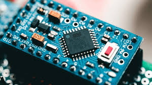
Surface Mount Technology is a method used to mount electronic components directly onto the surface of PCBs. Unlike traditional through-hole technology, where components are inserted into holes drilled in the PCB, SMT allows for a more compact design. This technology has become the standard in modern electronics due to its numerous advantages, including reduced size, weight, and manufacturing costs.
The Evolution of SMT
The development of SMT began in the 1960s, but it gained significant traction in the 1980s as the demand for smaller and more efficient electronic devices increased. The miniaturization of components and the advancement of automated assembly processes have made SMT a preferred choice for manufacturers. Today, SMT is widely used in various applications, from consumer electronics to automotive systems.
Benefits of SMT in PCB Design Efficiency
1. Reduced Size and Weight
One of the most significant advantages of SMT is its ability to reduce the size and weight of PCBs. By allowing components to be mounted directly on the surface, SMT eliminates the need for long leads, which can take up valuable space. This compact design is crucial for modern devices, where space is often at a premium. Smaller PCBs can lead to lighter products, which is particularly important in industries such as aerospace and mobile technology.
2. Higher Component Density
SMT enables a higher component density on PCBs. This means that more components can be placed in a smaller area, which is essential for complex electronic devices. Higher component density allows for more functionality within the same footprint, leading to innovative designs and improved performance. This is particularly beneficial in applications such as smartphones and tablets, where multiple functions are integrated into a single device.
3. Improved Electrical Performance
The shorter leads used in SMT reduce the inductance and capacitance associated with longer leads in through-hole components. This improvement in electrical performance is critical for high-frequency applications, where signal integrity is paramount. SMT components can handle higher frequencies and provide better overall performance, making them ideal for telecommunications and high-speed computing applications.
4. Faster Assembly Processes
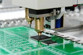
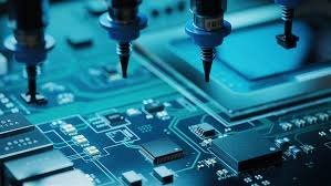
SMT significantly speeds up the assembly process. Automated pick-and-place machines can quickly and accurately place components on the PCB, reducing labor costs and assembly time. This efficiency is particularly important in high-volume production environments, where time-to-market is a critical factor. The ability to automate the assembly process also minimizes human error, leading to higher quality products.
5. Cost-Effectiveness
The cost-effectiveness of SMT is another reason for its widespread adoption. The reduction in PCB size and weight can lead to lower material costs, while the faster assembly processes reduce labor costs. Additionally, the ability to use smaller components can lead to savings in shipping and handling. Overall, SMT can significantly lower the total cost of production, making it an attractive option for manufacturers.

Challenges of Implementing SMT
While SMT offers numerous benefits, it is not without its challenges. Manufacturers must consider several factors when implementing SMT in their PCB designs.
1. Thermal Management
One of the challenges of SMT is managing heat dissipation. As components become smaller and more densely packed, the heat generated during operation can become a concern. Effective thermal management strategies, such as heat sinks and thermal vias, must be incorporated into the PCB design to ensure reliable operation.
2. Design Complexity
The increased component density and complexity of SMT designs can pose challenges for engineers. Designing PCBs with SMT requires a thorough understanding of the technology and careful planning to avoid issues such as signal integrity problems and manufacturing defects. Engineers must be well-versed in SMT design rules and best practices to ensure successful implementation.
3. Inspection and Testing
The small size of SMT components can make inspection and testing more challenging. Traditional visual inspection methods may not be sufficient, and manufacturers often rely on automated optical inspection (AOI) systems to detect defects. Ensuring that the assembly process is robust and that quality control measures are in place is essential for maintaining product reliability.
The Future of SMT in PCB Design
As technology continues to advance, the role of SMT in PCB design will only grow. Emerging trends such as the Internet of Things (IoT), wearable technology, and 5G communications are driving the demand for smaller, more efficient electronic devices. SMT will play a crucial role in meeting these demands, enabling manufacturers to create innovative products that push the boundaries of what is possible.
1. Integration with Advanced Technologies
The integration of SMT with advanced technologies such as artificial intelligence (AI) and machine learning will further enhance PCB design efficiency. These technologies can optimize the design process, improve manufacturing processes, and enable predictive maintenance, leading to higher quality products and reduced downtime.
2. Sustainability Considerations
As the electronics industry moves towards more sustainable practices, SMT will be at the forefront of these efforts. The reduction in material usage and the ability to design smaller, more efficient devices align with sustainability goals. Manufacturers will increasingly focus on eco-friendly materials and processes, making SMT an essential component of sustainable electronics manufacturing.
Conclusion
Surface Mount Technology has transformed the landscape of PCB design and manufacturing. Its ability to improve design efficiency through reduced size, higher component density, and faster assembly processes makes it a vital technology in the electronics industry. While challenges remain, the future of SMT looks promising, with advancements in technology and a growing emphasis on sustainability driving its evolution. As manufacturers continue to embrace SMT, we can expect to see even more innovative and efficient electronic devices in the years to come.

Related Questions
1. What is the difference between SMT and through-hole technology?
SMT involves mounting components directly on the surface of PCBs, while through-hole technology requires components to be inserted into drilled holes. SMT allows for smaller, more compact designs and higher component density.
2. How does SMT affect the cost of PCB manufacturing?
SMT can reduce manufacturing costs by minimizing material usage, speeding up assembly processes, and lowering labor costs. The compact design also leads to savings in shipping and handling.
3. What are the common challenges faced when using SMT?
Common challenges include thermal management, design complexity, and inspection difficulties. Effective strategies must be implemented to address these issues and ensure reliable operation.
4. How can manufacturers ensure quality control in SMT processes?
Manufacturers can implement automated optical inspection (AOI) systems, establish robust assembly processes, and adhere to best practices in SMT design to maintain high quality and reliability.
5. What future trends are expected in SMT technology?
Future trends include integration with advanced technologies like AI, a focus on sustainability, and continued miniaturization of components to meet the demands of emerging applications such as IoT and 5G.


