Content Menu
● Introduction
● Understanding PCB Manufacturing
>> What is PCB Manufacturing?
>> The Role of SMT in PCB Manufacturing
● The Wholesale PCB SMT Solution Line
>> Components of an SMT Line
>> How SMT Lines Reduce Defects
>>> 1. Automation and Precision
>>> 2. Real-Time Monitoring
>>> 3. Enhanced Inspection Techniques
>>> 4. Process Control
>>> 5. Continuous Improvement
● Benefits of Using a Wholesale PCB SMT Solution Line
>> Cost Efficiency
>> Improved Quality
>> Faster Time to Market
>> Scalability
● Detailed Examination of SMT Components
>> Solder Paste Printer
>> Pick and Place Machine
>> Reflow Oven
>> Inspection Systems
>> Cleaning Stations
● Challenges in PCB Manufacturing and How SMT Addresses Them
>> Common Defects in PCB Manufacturing
>> How SMT Addresses These Challenges
● Future Trends in PCB Manufacturing
>> Increased Automation
>> Smart Manufacturing
>> Sustainable Practices
● Conclusion
● FAQ
>> 1. What is the main advantage of using SMT in PCB manufacturing?
>> 2. How does automation in SMT lines reduce defects?
>> 3. What types of inspection are used in SMT lines?
>> 4. How can manufacturers ensure continuous improvement in their SMT processes?
>> 5. What impact does reducing defects have on production costs?
Introduction
In the rapidly evolving world of electronics, the demand for high-quality printed circuit boards (PCBs) is at an all-time high. As manufacturers strive to meet this demand, the implementation of Surface Mount Technology (SMT) has become a cornerstone of PCB production. A wholesale PCB SMT solution line is designed to enhance efficiency and reduce defects in the manufacturing process. This article explores how these systems work, the benefits they offer, and the critical role they play in ensuring the quality of PCBs.

Understanding PCB Manufacturing
What is PCB Manufacturing?
PCB manufacturing involves the creation of printed circuit boards that serve as the backbone for electronic devices. These boards are made from insulating materials, typically fiberglass, and are embedded with conductive pathways that connect various electronic components. The manufacturing process includes several stages, such as design, fabrication, assembly, and testing.
The Role of SMT in PCB Manufacturing
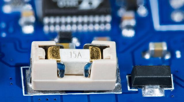
Surface Mount Technology (SMT) is a method used to mount electronic components directly onto the surface of PCBs. This technology has revolutionized PCB manufacturing by allowing for more compact designs and higher component density. SMT eliminates the need for drilling holes in the PCB, which not only saves time but also reduces the risk of defects associated with traditional through-hole technology.
The Wholesale PCB SMT Solution Line
Components of an SMT Line
A wholesale PCB SMT solution line typically consists of several key components:
1. Solder Paste Printer: This machine applies solder paste to the PCB in precise locations where components will be placed.
2. Pick and Place Machine: This automated system picks up components from reels or trays and places them onto the PCB.
3. Reflow Oven: After placement, the PCB passes through a reflow oven where the solder paste is melted, creating a strong bond between the components and the board.
4. Inspection Systems: Automated optical inspection (AOI) and X-ray machines are used to detect defects in the assembly process.
5. Cleaning Stations: These stations remove any residual flux or contaminants from the PCB after soldering.
How SMT Lines Reduce Defects
1. Automation and Precision
The automation of the SMT process significantly reduces human error, which is a common source of defects in PCB manufacturing. Machines are programmed to perform tasks with high precision, ensuring that components are placed accurately and soldered correctly. This level of automation minimizes variations that can lead to defects.
2. Real-Time Monitoring
Modern SMT lines are equipped with real-time monitoring systems that track the manufacturing process. These systems can detect anomalies and alert operators immediately, allowing for quick corrective actions. This proactive approach helps to identify and rectify potential defects before they escalate.
3. Enhanced Inspection Techniques
The integration of advanced inspection technologies, such as AOI and X-ray inspection, allows for thorough examination of the PCBs at various stages of production. These systems can identify defects such as misaligned components, insufficient solder, and other issues that may not be visible to the naked eye. Early detection of these defects is crucial for maintaining quality.
4. Process Control
Implementing strict process control measures is essential in reducing defects. This includes standardizing procedures, maintaining equipment, and conducting regular training for operators. By ensuring that every aspect of the manufacturing process is controlled and monitored, manufacturers can significantly reduce the likelihood of defects.
5. Continuous Improvement
Wholesale PCB SMT solution lines often incorporate feedback loops that allow for continuous improvement. Data collected during the manufacturing process can be analyzed to identify trends and areas for improvement. This iterative process helps manufacturers refine their operations and reduce defects over time.
Benefits of Using a Wholesale PCB SMT Solution Line
Cost Efficiency
By reducing defects, manufacturers can lower their production costs. Fewer defects mean less rework and fewer materials wasted, leading to significant savings. Additionally, the efficiency of automated systems allows for higher production rates, further enhancing cost-effectiveness.
Improved Quality
The primary goal of any manufacturing process is to produce high-quality products. A wholesale PCB SMT solution line enhances the quality of PCBs by minimizing defects and ensuring that each board meets stringent quality standards. This reliability is crucial for manufacturers who depend on PCBs for their electronic devices.
Faster Time to Market
With increased efficiency and reduced defects, manufacturers can bring their products to market faster. This speed is essential in the competitive electronics industry, where being first to market can provide a significant advantage.
Scalability
Wholesale PCB SMT solution lines are designed to be scalable, allowing manufacturers to adjust their production capacity based on demand. This flexibility is vital for businesses that need to respond quickly to market changes.
Detailed Examination of SMT Components
Solder Paste Printer
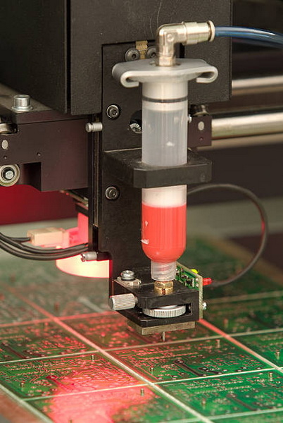
The solder paste printer is a critical component of the SMT line. It ensures that the right amount of solder paste is applied to the PCB. The printer uses a stencil to accurately deposit solder paste onto the pads where components will be placed. This precision is vital because too much or too little solder can lead to defects such as solder bridges or cold solder joints. Advanced printers are equipped with vision systems that verify the accuracy of the paste application, further reducing the risk of defects.
Pick and Place Machine
The pick and place machine is responsible for placing components onto the PCB. This machine uses a combination of vacuum and mechanical arms to pick components from their packaging and place them onto the correct locations on the board. The speed and accuracy of these machines are crucial; modern pick and place machines can place thousands of components per hour with high precision. Some machines are equipped with advanced vision systems that allow them to identify and correct placement errors in real-time.

Reflow Oven
The reflow oven is where the solder paste is melted to create a permanent bond between the components and the PCB. The oven uses a controlled heating profile to ensure that the solder reaches the appropriate temperature for melting and then cools down at a controlled rate to avoid thermal shock. Proper reflow is essential for preventing defects such as solder voids and insufficient solder connections. Manufacturers often conduct extensive profiling to optimize the reflow process for different types of solder and components.
Inspection Systems
Inspection systems are vital for maintaining quality in PCB manufacturing. Automated optical inspection (AOI) systems use cameras to capture images of the PCB and compare them to a reference image to identify defects. X-ray inspection is used for detecting issues that are not visible on the surface, such as solder joint integrity in BGA (Ball Grid Array) components. These inspection systems can operate at high speeds, allowing for real-time feedback and immediate corrective actions.
Cleaning Stations
After soldering, PCBs may have residual flux or contaminants that need to be removed. Cleaning stations use various methods, including ultrasonic cleaning and solvent cleaning, to ensure that the boards are free from any residues that could affect performance or reliability. Proper cleaning is essential for preventing issues such as corrosion and electrical shorts.
Challenges in PCB Manufacturing and How SMT Addresses Them
Common Defects in PCB Manufacturing
Despite advancements in technology, PCB manufacturing is not without its challenges. Common defects include:
- Solder Bridges: These occur when excess solder creates an unintended connection between two or more pads.
- Cold Solder Joints: These are weak connections that occur when solder does not melt properly during the reflow process.
- Misalignment: This defect happens when components are not placed accurately on the PCB, leading to poor electrical connections.
- Component Damage: Components can be damaged during handling or placement, especially if they are sensitive to heat or mechanical stress.
How SMT Addresses These Challenges
SMT technology addresses these challenges through its automated processes and advanced inspection techniques. For instance, the precision of the pick and place machines minimizes the risk of misalignment, while the controlled environment of the reflow oven reduces the likelihood of cold solder joints. Additionally, real-time monitoring and inspection systems help identify defects early in the process, allowing for immediate corrective actions.
Future Trends in PCB Manufacturing
Increased Automation
The trend towards increased automation in PCB manufacturing is expected to continue. As technology advances, manufacturers will adopt more sophisticated machines that can operate with minimal human intervention. This shift will further reduce defects and improve efficiency.
Smart Manufacturing
The integration of IoT (Internet of Things) technologies into PCB manufacturing is another emerging trend. Smart manufacturing systems can collect and analyze data from various stages of production, providing insights that can lead to further improvements in quality and efficiency.
Sustainable Practices
As environmental concerns grow, manufacturers are increasingly focusing on sustainable practices. This includes reducing waste, using eco-friendly materials, and implementing energy-efficient processes. SMT lines can contribute to sustainability by minimizing material waste and improving energy efficiency.
Conclusion
In conclusion, a wholesale PCB SMT solution line plays a critical role in reducing defects in PCB manufacturing. Through automation, real-time monitoring, enhanced inspection techniques, strict process control, and a commitment to continuous improvement, these systems ensure that manufacturers can produce high-quality PCBs efficiently and cost-effectively. As the demand for electronic devices continues to grow, the importance of reliable and defect-free PCBs cannot be overstated. The future of PCB manufacturing looks promising, with advancements in technology paving the way for even greater efficiency and quality.

FAQ
1. What is the main advantage of using SMT in PCB manufacturing?
The main advantage of using SMT is the ability to place components directly on the surface of the PCB, allowing for more compact designs and higher component density, which leads to improved performance and reduced manufacturing costs.
2. How does automation in SMT lines reduce defects?
Automation reduces defects by minimizing human error, ensuring precise placement of components, and maintaining consistent quality throughout the manufacturing process.
3. What types of inspection are used in SMT lines?
Common types of inspection used in SMT lines include automated optical inspection (AOI), X-ray inspection, and visual inspection to detect defects such as misalignment and insufficient solder.
4. How can manufacturers ensure continuous improvement in their SMT processes?
Manufacturers can ensure continuous improvement by analyzing data collected during production, identifying trends, and implementing changes based on feedback to refine their processes.
5. What impact does reducing defects have on production costs?
Reducing defects leads to lower production costs by minimizing rework, reducing material waste, and increasing overall efficiency, allowing manufacturers to save money and improve profitability.


