Content Menu
● Understanding SMT PCB Pads
>> Key Functions of SMT PCB Pads
● How SMT PCB Pads Enhance Circuit Board Performance
>> 1. Improved Electrical Performance
>> 2. Superior Thermal Management
>> 3. Enhanced Manufacturing Efficiency
>> 4. Design Flexibility and Miniaturization
>> 5. Improved Reliability and Durability
● Best Practices for SMT PCB Pad Design
>> Pad Size and Shape
>> Surface Finish
>> Thermal Relief
>> Solder Mask Design
>> Design Rule Checks (DRC)
● Additional Considerations for SMT PCB Pads
>> Impact on Signal Integrity
>> Environmental and Mechanical Factors
>> Compatibility with Lead-Free Soldering
● Conclusion
● FAQ
>> 1. What is the primary function of an SMT PCB pad?
>> 2. How do SMT PCB pads improve thermal management?
>> 3. Why are SMT PCB pads better for high-frequency circuits?
>> 4. How do SMT PCB pads aid automated manufacturing?
>> 5. Can SMT PCB pads support miniaturized components?
Surface Mount Technology (SMT) has revolutionized the design and manufacturing of printed circuit boards (PCBs), enabling more compact, efficient, and high-performance electronic devices. At the heart of SMT's success are SMT PCB pads, which serve as the critical interface between surface mount devices (SMDs) and the circuit board. This article explores how SMT PCB pads enhance circuit board performance by improving electrical connectivity, thermal management, manufacturing efficiency, and overall reliability.

Understanding SMT PCB Pads
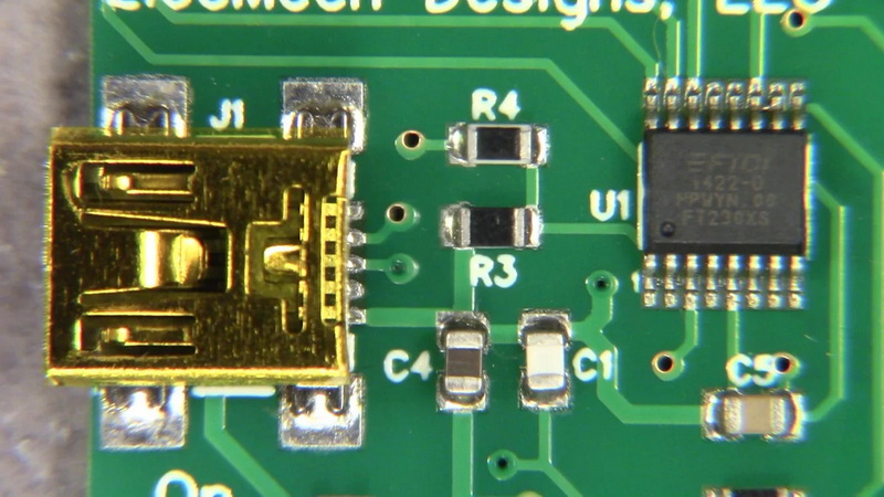
SMT PCB pads are small conductive areas on the surface of a PCB designed specifically to mount surface mount components. Unlike through-hole pads that require drilling holes for component leads, SMT pads provide a flat surface for soldering components directly onto the PCB.
Key Functions of SMT PCB Pads
- Electrical Connection: SMT pads ensure reliable electrical contact between the PCB traces and the component terminals.
- Mechanical Support: They provide mechanical anchoring for components to withstand vibration and mechanical stresses.
- Thermal Management: Properly designed pads aid in dissipating heat generated by components, which is crucial for maintaining performance and longevity.
- Manufacturing Facilitation: SMT pads are optimized for automated pick-and-place and soldering processes, enhancing production speed and yield.
How SMT PCB Pads Enhance Circuit Board Performance
1. Improved Electrical Performance
SMT PCB pads contribute to enhanced electrical performance by minimizing lead lengths and parasitic effects such as capacitance and inductance. Shorter interconnections reduce signal delay and electromagnetic interference (EMI), which is particularly important in high-frequency and high-speed circuits.
- The compact design of SMT pads allows for shorter signal paths, improving signal integrity and reducing noise.
- Reduced lead inductance and resistance on SMT pads mitigate RF interference, enabling better electromagnetic compatibility (EMC).
- SMT pads also enable precise impedance control in high-speed digital and RF circuits by maintaining consistent pad dimensions and spacing, which is critical for signal integrity.
2. Superior Thermal Management
Thermal management is critical in preventing component overheating and ensuring long-term reliability. SMT PCB pads can be designed with optimized size and shape to improve heat dissipation.
- Larger or thermal relief pads help spread and dissipate heat away from components effectively.
- Proper pad design reduces hotspots and maintains stable operating temperatures, enhancing circuit durability.
- Thermal vias connected to SMT pads can channel heat to inner or opposite layers of the PCB, improving overall thermal conductivity.
- Heat dissipation through SMT pads also helps maintain solder joint integrity, preventing thermal fatigue and failures in harsh operating environments.
3. Enhanced Manufacturing Efficiency
SMT PCB pads are integral to automated assembly processes, significantly increasing production efficiency and reducing costs.
- SMT pads eliminate the need for drilling holes, simplifying PCB fabrication and reducing material waste.
- The flat surface of SMT pads facilitates precise solder paste application and component placement by automated machines, enabling high-speed assembly lines.
- The surface tension of molten solder during reflow soldering helps self-align components on SMT pads, correcting minor placement errors automatically.
- SMT pads reduce the complexity of PCB assembly by supporting a wide range of component sizes and types, from tiny 0201 resistors to larger ICs, all on the same board.
- The elimination of through-holes also reduces the risk of solder wicking and solder joint defects, improving overall yield.
4. Design Flexibility and Miniaturization
SMT PCB pads enable higher component density and flexible PCB layouts, which are essential for modern compact electronics.
- Components can be mounted on both sides of the PCB using SMT pads, doubling the available space for circuitry.
- Smaller pad sizes support miniaturized components, allowing for lighter, thinner, and more compact devices such as smartphones and wearables.
- SMT pads support complex and high-density interconnections, enabling advanced circuit designs.
- The ability to place components closer together reduces the overall PCB size, which lowers material costs and improves electrical performance by shortening trace lengths.
- SMT pad design can be customized for specific components, such as fine-pitch ICs, BGA packages, and QFN types, allowing for advanced packaging solutions and integration.
5. Improved Reliability and Durability
The mechanical and electrical stability provided by SMT PCB pads enhances the overall reliability of the circuit board.
- SMT pads provide strong solder joints that resist vibration and mechanical shocks better than through-hole counterparts.
- The overlapping solder mask around SMT pads prevents pad shifting or detachment during assembly and operation, ensuring long-term durability.
- Proper pad design minimizes the risk of solder joint cracks caused by thermal cycling or mechanical stress.
- SMT pads also reduce the likelihood of solder bridging and tombstoning defects during reflow soldering, improving the reliability of the assembled PCB.
- The use of robust pad finishes such as ENIG (Electroless Nickel Immersion Gold) further enhances corrosion resistance and solderability, prolonging the life of the PCB.

Best Practices for SMT PCB Pad Design
To maximize the benefits of SMT PCB pads, careful design considerations are essential. The following best practices help ensure optimal pad performance:
Pad Size and Shape
- Pads must be sized to match component leads precisely. Oversized pads can cause solder bridging, while undersized pads may lead to weak solder joints.
- Rectangular or rounded pad shapes are preferred depending on component type and soldering method.
- For fine-pitch components, pad dimensions should comply with IPC standards to avoid solder defects.
Surface Finish
- The choice of surface finish affects solderability and long-term reliability.
- Common finishes include HASL (Hot Air Solder Leveling), ENIG, OSP (Organic Solderability Preservative), and Immersion Silver.
- ENIG is preferred for fine-pitch SMT pads due to its flat surface and excellent oxidation resistance.
Thermal Relief
- Incorporating thermal relief patterns in pads connected to large copper pours helps balance heat dissipation and soldering ease.
- Thermal vias placed near SMT pads improve heat conduction to inner PCB layers.
- Careful thermal design prevents overheating and ensures consistent solder joint quality.
Solder Mask Design
- Proper solder mask clearance around SMT pads prevents solder bridging and shorts.
- Solder mask-defined (SMD) pads provide better control over pad dimensions and reduce copper exposure.
- Mask openings should be aligned precisely with pads to avoid manufacturing defects.
Design Rule Checks (DRC)
- PCB design software tools offer DRC features to verify pad spacing, alignment, and sizing.
- Following IPC-7351 standards ensures compatibility with industry-accepted SMT pad designs.
- Regular design reviews and simulations help identify potential issues before manufacturing.
Additional Considerations for SMT PCB Pads
Impact on Signal Integrity
In high-speed digital and RF circuits, the geometry of SMT PCB pads can significantly influence signal integrity. Variations in pad size and shape can introduce impedance discontinuities, reflections, and crosstalk. Engineers must carefully model and simulate pad effects during the PCB design phase to ensure optimal performance.
Environmental and Mechanical Factors
SMT PCB pads must withstand environmental stresses such as humidity, temperature cycling, and mechanical vibration. The choice of pad finish, solder alloy, and pad design all contribute to the board's ability to maintain performance under harsh conditions. For example, ENIG finish pads resist corrosion better in humid environments, enhancing long-term reliability.
Compatibility with Lead-Free Soldering
With the global shift toward lead-free soldering, SMT PCB pads must be compatible with higher reflow temperatures and different solder alloys. Pad materials and finishes should be selected to maintain solderability and prevent oxidation during lead-free soldering processes.
Conclusion
SMT PCB pads play a pivotal role in enhancing circuit board performance by improving electrical connectivity, thermal management, manufacturing efficiency, design flexibility, and reliability. Their optimized design enables the production of compact, high-speed, and durable electronic devices essential for modern technology. As SMT continues to dominate PCB assembly, understanding and implementing effective SMT PCB pad design is critical for engineers and manufacturers striving for superior circuit board quality and performance.
By adhering to best design practices and considering environmental and manufacturing factors, SMT PCB pads can unlock the full potential of surface mount technology, driving innovation in electronics across industries.

FAQ
1. What is the primary function of an SMT PCB pad?
SMT PCB pads provide the electrical and mechanical interface for surface mount components, enabling reliable solder joints and stable connections on the PCB surface.
2. How do SMT PCB pads improve thermal management?
By optimizing pad size, shape, and incorporating thermal relief features, SMT pads help dissipate heat away from components, preventing overheating and improving circuit reliability.
3. Why are SMT PCB pads better for high-frequency circuits?
They reduce lead lengths and parasitic inductance and capacitance, minimizing signal delay and electromagnetic interference, which enhances signal integrity in high-frequency applications.
4. How do SMT PCB pads aid automated manufacturing?
Their flat, hole-free design allows precise solder paste application and automated pick-and-place assembly, increasing production speed, reducing errors, and lowering manufacturing costs.
5. Can SMT PCB pads support miniaturized components?
Yes, SMT pads can be designed in very small sizes to accommodate miniature components, enabling compact and lightweight PCB designs for modern electronics like smartphones and wearables.


