Content Menu
● Understanding SMD Inspection Machines
● Key Technologies in SMD Inspection Machines
>> 1. Solder Paste Inspection (SPI)
>> 2. Automated Optical Inspection (AOI)
>> 3. Automated X-ray Inspection (AXI)
● How SMD Inspection Machines Detect Hidden Soldering Issues
>> Multi-Angle and 3D Imaging
>> Advanced Image Processing and AI
>> Multi-Color LED Lighting and High-Resolution Cameras
>> Integration with SMT Production Lines
● Benefits of Using SMD Inspection Machines for Hidden Soldering Issue Detection
● Conclusion
● FAQ
>> 1. What types of defects can an SMD inspection machine detect?
>> 2. How does solder paste inspection (SPI) differ from automated optical inspection (AOI)?
>> 3. Why is X-ray inspection important in SMD inspection?
>> 4. How does AI improve the performance of SMD inspection machines?
>> 5. Can SMD inspection machines be integrated into SMT production lines?
● Citations:
Surface Mount Device (SMD) inspection machines are essential tools in modern electronics manufacturing, ensuring the quality and reliability of printed circuit boards (PCBs). These machines play a crucial role in detecting hidden soldering issues that are often difficult or impossible to identify through manual inspection alone. This article explores how SMD inspection machines work, the technologies they employ, and their importance in maintaining high-quality solder joints in Surface Mount Technology (SMT) assembly.

Understanding SMD Inspection Machines
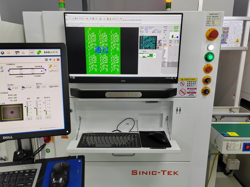
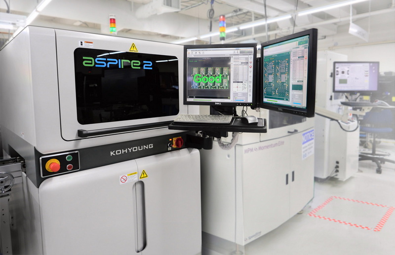
An SMD inspection machine is an automated system designed to inspect PCBs during or after the surface mount assembly process. Its primary function is to detect defects in solder joints and component placement that could lead to product failure. These machines use various inspection technologies, including:
- Solder Paste Inspection (SPI)
- Automated Optical Inspection (AOI)
- Automated X-ray Inspection (AXI)
Each technology targets specific aspects of the soldering process and component placement to ensure comprehensive defect detection.
Key Technologies in SMD Inspection Machines
1. Solder Paste Inspection (SPI)
SPI machines measure the solder paste's volume, height, and area on the PCB pads before component placement. By using 3D imaging techniques, these machines can detect:
- Insufficient solder paste
- Excessive solder paste
- Misaligned or missing solder paste deposits
Early detection of these issues is critical because improper solder paste application can cause poor solder joints, leading to electrical failures[1][3][9].
2. Automated Optical Inspection (AOI)
AOI machines use high-resolution cameras and advanced image processing algorithms to inspect solder joints and component placement after reflow soldering. The AOI system compares the captured images against a reference model to identify:
- Solder bridges (short circuits)
- Missing or misaligned components
- Solder splashes and balls
- Open solder joints or insufficient solder
- Bent or damaged leads
AOI inspection is fast, non-contact, and capable of inspecting complex assemblies with high accuracy, making it ideal for inline production quality control[2][6][7].
3. Automated X-ray Inspection (AXI)
AXI machines use X-ray imaging to penetrate the PCB and reveal hidden solder joints beneath components like Ball Grid Arrays (BGAs) and other packages with concealed leads. This technology can detect:
- Voids and cracks inside solder joints
- Insufficient solder volume
- Misalignment of hidden components
- Internal solder defects not visible to optical systems
AXI complements AOI by providing a non-destructive method to inspect hidden soldering issues that are otherwise undetectable[6][7].

How SMD Inspection Machines Detect Hidden Soldering Issues
Multi-Angle and 3D Imaging
Modern SMD inspection machines utilize multi-angle cameras and 3D imaging to capture detailed views of solder joints from different perspectives. This allows the detection of subtle defects such as:
- Tombstoning (where one end of a component lifts off the pad)
- Solder joint fillet shape anomalies
- Voids and insufficient solder volume
3D solder paste inspection machines, in particular, measure the height and volume of solder paste deposits, ensuring that the soldering process will produce reliable joints[1][3][9].
Advanced Image Processing and AI
Many SMD inspection machines incorporate artificial intelligence (AI) and machine learning algorithms to enhance defect detection accuracy. For example, systems like SolderNet use explainable AI to identify solder joint defects with transparency and trustworthiness, reducing false positives and improving inspection reliability[8].
These AI-driven systems analyze image features such as texture, shape, and color variations to detect defects that may escape traditional rule-based inspection methods.
Multi-Color LED Lighting and High-Resolution Cameras
The use of multi-color LED lighting and high-resolution color cameras improves defect visibility by enhancing contrast and revealing subtle soldering problems such as solder splashes, bridges, and small solder balls. This lighting technique helps in capturing clear meniscus shapes and short circuits, which are critical for solder joint quality assessment[5].
Integration with SMT Production Lines
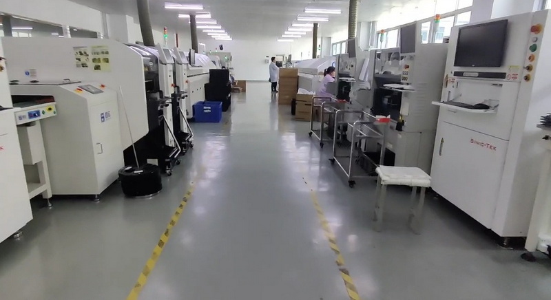
SMD inspection machines are often integrated directly into SMT production lines, allowing for real-time inspection and immediate feedback. This integration enables:
- Rapid detection and correction of defects
- Closed-loop process control to optimize soldering parameters
- Reduction of rework and scrap rates
By detecting hidden soldering issues early, manufacturers can prevent costly downstream failures and improve overall product quality[9].
Benefits of Using SMD Inspection Machines for Hidden Soldering Issue Detection
- Improved Quality Assurance: Automated inspection provides consistent, objective, and reproducible results, reducing human error inherent in manual inspections[5][6].
- Early Defect Detection: Identifying defects such as insufficient solder, misalignment, and solder bridges before final assembly prevents product failures and costly recalls[9].
- Increased Production Efficiency: Automated systems inspect PCBs rapidly, enabling high throughput without compromising accuracy[7].
- Comprehensive Defect Coverage: Combining SPI, AOI, and AXI technologies ensures detection of both visible and hidden soldering defects[7].
- Data-Driven Process Optimization: Inspection data helps optimize soldering processes, reducing defects and improving yield[5].
Conclusion
SMD inspection machines are indispensable in modern electronics manufacturing for detecting hidden soldering issues that compromise product reliability. By leveraging advanced imaging technologies such as 3D solder paste inspection, automated optical inspection, and X-ray inspection, these machines provide comprehensive and accurate defect detection. The integration of AI further enhances their capability to identify subtle defects with high confidence. Ultimately, SMD inspection machines ensure high-quality solder joints, reduce rework and scrap, and contribute to the production of reliable electronic devices.

FAQ
1. What types of defects can an SMD inspection machine detect?
SMD inspection machines can detect a wide range of defects including insufficient or excessive solder paste, solder bridges, missing or misaligned components, solder splashes, open solder joints, bent leads, voids inside solder joints, and hidden defects under components like BGAs[1][2][5][6].
2. How does solder paste inspection (SPI) differ from automated optical inspection (AOI)?
SPI focuses on measuring the solder paste volume, height, and area before component placement using 3D imaging, ensuring proper solder paste application. AOI inspects the solder joints and component placement after reflow soldering using high-resolution cameras and image processing to detect soldering and placement defects[1][2][3].
3. Why is X-ray inspection important in SMD inspection?
X-ray inspection is crucial for detecting hidden soldering defects beneath components with concealed leads, such as BGAs. It reveals internal voids, cracks, and insufficient solder volume that optical systems cannot see, providing a non-destructive way to ensure solder joint integrity[6][7].
4. How does AI improve the performance of SMD inspection machines?
AI and machine learning algorithms enhance defect detection accuracy by analyzing complex image features and patterns beyond simple rule-based methods. AI systems like SolderNet provide explainable and trustworthy defect identification, reducing false positives and improving inspection reliability[8].
5. Can SMD inspection machines be integrated into SMT production lines?
Yes, SMD inspection machines are often integrated inline within SMT production lines, enabling real-time inspection and immediate feedback for process optimization. This integration helps reduce defects, rework, and production costs while improving overall quality[7][9].
Citations:
[1] https://ascinternational.com/3d-spi/what-is-a-solder-paste-inspection-machine/
[2] https://htgdmachine.en.made-in-china.com/product/IFZfrmQcgAkS/China-PCB-Soldering-Tester-SMT-Aoi-SMD-Inspection-Machine.html
[3] https://smtmachineline.com/smt-spi-solder-paste-inspection-machine/
[4] https://ntrs.nasa.gov/api/citations/19930016948/downloads/19930016948.pdf
[5] https://www.modus-hightech.com/solutions/tht-soldering-inspection/
[6] https://www.mtek.co.uk/different-types-of-surface-mount-technology-inspection
[7] https://core-emt.com/inspection
[8] https://onlinelibrary.wiley.com/doi/full/10.1002/aaai.12129
[9] https://www.jt-int.com/benefits-of-a-3d-solder-paste-inspection-machine/
[10] https://www.linkedin.com/pulse/importance-types-smt-inspection-electronics-manufacturing-rzfac
[11] https://pmc.ncbi.nlm.nih.gov/articles/PMC9228397/
[12] https://www.neodensmt.com/news/what-inspection-equipment-is-needed-for-smt-as-75421941.html
[13] https://vicoimaging.com/smd-and-smt-comprehensive-guide/


