Content Menu
● The Importance of SMT Components
● Design Phase
>> Schematic Design
>> PCB Layout
>> Design Review
● Component Fabrication
>> Material Selection
>> Manufacturing Processes
>> Quality Control
● Assembly Process
>> Solder Paste Application
>> Component Placement
>> Reflow Soldering
>> Inspection
● Testing Phase
>> Functional Testing
>> In-Circuit Testing (ICT)
>> Burn-In Testing
● Future Trends in SMT Component Manufacturing
>> Miniaturization
>> Advanced Materials
>> Automation and AI Integration
>> Sustainability Initiatives
● Conclusion
● FAQ
>> 1. What are SMT components?
>> 2. What advantages do SMT components have over traditional through-hole components?
>> 3. How does reflow soldering work?
>> 4. What types of tests are performed on SMT assemblies?
>> 5. Why is quality control important in SMT component manufacturing?
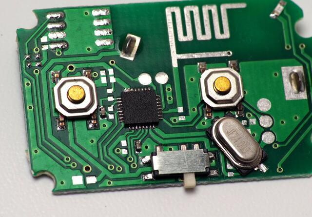
Surface Mount Technology (SMT) is a method used to produce electronic circuits in which the components are mounted directly onto the surface of printed circuit boards (PCBs). This technology has revolutionized the electronics manufacturing industry due to its efficiency, compactness, and cost-effectiveness. Understanding how SMT components are made involves examining various stages, including design, component fabrication, assembly, and testing. This article delves into each of these stages in detail.

The Importance of SMT Components
SMT components are critical in modern electronics. They allow for smaller and lighter devices, which are essential in today's technology-driven world. The benefits of SMT include:
- Reduced Size: SMT components are typically smaller than their through-hole counterparts, allowing for more compact designs.
- Higher Component Density: More components can be placed on a single PCB, leading to increased functionality without enlarging the device.
- Improved Performance: Shorter connections between components reduce signal loss and improve overall performance.
- Cost Efficiency: The automated assembly processes associated with SMT can lower labor costs and increase production speed.
- Enhanced Reliability: SMT components often have better resistance to shock and vibration due to their solid mounting on the PCB.
Design Phase
The creation of SMT components begins with the design phase. This stage is crucial as it lays the foundation for all subsequent processes.
Schematic Design
The first step involves creating a schematic diagram that represents the electronic circuit. Engineers use specialized software to design the circuit, ensuring that all components are correctly represented and connected. This software often includes libraries of standard components, making it easier for engineers to select appropriate parts for their designs.
PCB Layout
Once the schematic is complete, the next step is to create a PCB layout. This involves placing the components on the board in a way that optimizes space and minimizes interference. Key considerations during this phase include:
- Component Placement: Components must be strategically placed to facilitate efficient routing of electrical connections. Designers often use guidelines such as keeping high-frequency components away from noisy power supplies or ensuring adequate spacing for thermal management.
- Signal Integrity: Designers must consider factors such as impedance and crosstalk to ensure optimal performance. This may involve using differential pairs for high-speed signals or implementing ground planes to shield sensitive traces.
- Thermal Management: Heat generated by components must be managed effectively to prevent damage or performance degradation. This can involve adding thermal vias or using heat sinks for high-power components.
Design Review
After completing the layout, a thorough design review is conducted. This step involves checking for errors or potential issues that could arise during manufacturing or operation. Engineers often use simulation tools to predict how the circuit will behave under various conditions. Additionally, peer reviews among team members can help catch mistakes that one individual might overlook.
Component Fabrication
With the design finalized, the next step is component fabrication. This process involves producing the individual SMT components that will be mounted on the PCB.
Material Selection
The choice of materials is critical in component fabrication. Common materials include:
- Ceramics: Used for capacitors and resistors due to their stability and reliability under varying temperatures and voltages.
- Metals: Such as copper and aluminum for conductive paths; copper is particularly favored due to its excellent conductivity.
- Polymers: Employed in various applications for insulation and protection, particularly in flexible circuits.
Manufacturing Processes
Different manufacturing processes are used depending on the type of component being produced:
- Thin Film Technology: Used for resistors and capacitors, this process involves depositing thin layers of material onto a substrate using techniques like sputtering or chemical vapor deposition (CVD).
- Thick Film Technology: Involves printing conductive pastes onto a substrate and firing it at high temperatures to create resistive elements. This method is commonly used for hybrid circuits where multiple technologies are combined.
- Die Attach and Wire Bonding: Used for integrated circuits (ICs), where silicon chips are attached to substrates using adhesives or soldering techniques. Wire bonding connects the chip pads to package leads using ultra-fine gold or aluminum wires.
Quality Control
Quality control is paramount during component fabrication. Various tests are performed to ensure that each component meets specified standards. These tests may include:
- Electrical Testing: To verify that components function correctly under specified conditions.
- Mechanical Testing: To assess durability and resistance to stress through methods such as tensile strength tests or drop tests.
- Environmental Testing: To evaluate performance under different temperature and humidity conditions, ensuring reliability in real-world applications.

Assembly Process
Once the components are fabricated, they must be assembled onto the PCB. The assembly process can be broken down into several key steps:
Solder Paste Application
The first step in assembly is applying solder paste to the PCB pads where components will be placed. Solder paste is a mixture of tiny solder balls and flux that helps create a strong electrical connection when heated. The application is typically done using stencil printing techniques that ensure precise placement of solder paste only where needed.
Component Placement
After applying solder paste, automated pick-and-place machines position SMT components onto the PCB pads. These machines use precise robotic arms equipped with vision systems to identify component orientation and ensure accurate placement, significantly reducing human error and increasing speed.
Reflow Soldering
Once all components are placed, the PCB undergoes reflow soldering. This process involves heating the board in an oven to melt the solder paste, creating permanent connections between components and pads. The reflow process typically consists of several stages:
- Preheat Stage: Gradually heats the board to prepare it for soldering while avoiding thermal shock.
- Soak Stage: Maintains a specific temperature to ensure uniform heating across all components before reaching reflow temperatures.
- Reflow Stage: The temperature peaks above solder melting point (usually around 217°C), melting the solder paste.
- Cooling Stage: Rapidly cools down the board to solidify the solder joints without introducing stress fractures.
Inspection
After reflow soldering, each PCB undergoes inspection to ensure that all components are correctly placed and soldered. Common inspection methods include:
- Automated Optical Inspection (AOI): Uses cameras to capture images of PCBs and identify defects such as missing components or misaligned parts.
- X-ray Inspection: Used for more complex assemblies where hidden solder joints need examination, particularly important for BGA (Ball Grid Array) packages where connections are not visible from above.
Testing Phase
The final stage in manufacturing SMT components is testing. This phase ensures that each assembled PCB functions as intended before it is shipped out for use.
Functional Testing
Functional testing verifies that each circuit operates according to its specifications. This may involve applying power to the board and checking outputs against expected values under various operating conditions.
In-Circuit Testing (ICT)
ICT tests individual components on a PCB while it is still assembled. Specialized fixtures connect directly to test points on the board, allowing engineers to measure voltages, currents, and resistances without disassembling anything. ICT can identify faulty parts quickly and efficiently before final assembly steps occur.
Burn-In Testing
Burn-in testing subjects PCBs to elevated temperatures or voltages over an extended period—often days—to identify early failures by stressing the components beyond typical operating conditions. This testing helps ensure long-term reliability in end-use applications by filtering out weak parts before they reach consumers.
Future Trends in SMT Component Manufacturing
As technology advances, several trends are shaping the future of SMT component manufacturing:
Miniaturization
As devices continue shrinking in size while increasing functionality, manufacturers are focusing on developing even smaller SMT components without compromising performance or reliability.
Advanced Materials
The development of new materials—such as flexible substrates—allows for innovative designs in wearables and other compact electronics where traditional rigid PCBs would not suffice.
Automation and AI Integration
Incorporating artificial intelligence into manufacturing processes can enhance quality control measures by predicting failures based on historical data patterns or optimizing production schedules dynamically based on demand forecasts.
Sustainability Initiatives
With growing environmental concerns, manufacturers are exploring eco-friendly materials and processes that reduce waste during production while improving recyclability at end-of-life stages for electronic devices.
Conclusion
The manufacturing of SMT components involves several intricate steps—from design through assembly and testing—each crucial for ensuring high-quality electronic products. As technology continues to evolve, so too will methods for producing these essential components, driving advancements in efficiency, miniaturization, and performance across various industries. Understanding this process not only highlights its complexity but also emphasizes its significance in our increasingly electronic world.

FAQ
1. What are SMT components?
SMT components are electronic parts designed for surface mount technology, allowing them to be mounted directly onto PCBs without needing holes drilled through them.
2. What advantages do SMT components have over traditional through-hole components?
SMT components offer several advantages including reduced size, higher density on PCBs, improved performance due to shorter electrical paths, lower manufacturing costs due to automation, enhanced reliability against physical stresses like shock or vibration, and better thermal management capabilities.
3. How does reflow soldering work?
Reflow soldering involves applying solder paste on PCB pads where SMT components will be placed; then heating them in an oven until the solder melts around each component lead creating permanent connections upon cooling down through controlled temperature profiles during different stages of heating cycles.
4. What types of tests are performed on SMT assemblies?
Common tests include functional testing (to check if circuits operate correctly), in-circuit testing (to test individual component functionality), burn-in testing (to identify early failures under stress), automated optical inspection (for visual defects), and X-ray inspection (for hidden joint verification).
5. Why is quality control important in SMT component manufacturing?
Quality control ensures that each component meets specified standards for performance and reliability; reducing defects leads not only improves customer satisfaction but also minimizes costly recalls or repairs after products reach consumers' hands.


