Content Menu
● Understanding SMT Prototyping
● The SMT Prototyping Process
● Advantages of SMT Prototyping
>> 1. Compact Design
>> 2. Improved Performance
>> 3. Higher Production Efficiency
>> 4. Cost-Effectiveness
>> 5. Enhanced Reliability
● Applications of SMT Prototyping
>> Consumer Electronics
>> Automotive Industry
>> Medical Devices
>> Industrial Automation
● Challenges in SMT Prototyping
>> 1. Design Complexity
>> 2. Thermal Management
>> 3. Component Availability
>> 4. Testing and Debugging
● Conclusion
● FAQ
>> 1. What is the main difference between SMT and through-hole technology?
>> 2. Why is SMT prototyping preferred for high-volume production?
>> 3. What industries benefit the most from SMT prototyping?
>> 4. What are the challenges associated with SMT prototyping?
>> 5. How can I ensure the reliability of SMT prototypes?
In the world of electronics, the design and manufacturing of printed circuit boards (PCBs) are crucial steps that determine the performance and reliability of electronic devices. As technology advances, the demand for more compact, efficient, and high-performance PCBs has led to the adoption of Surface Mount Technology (SMT) prototyping. This article explores the benefits of SMT prototyping for PCB design, the processes involved, and why it is a preferred choice for engineers and manufacturers alike.

Understanding SMT Prototyping
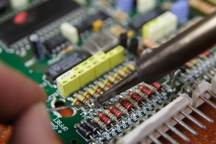
Surface Mount Technology (SMT) is a method used to mount electronic components directly onto the surface of a PCB. Unlike traditional through-hole technology, where components are inserted into holes and soldered on the opposite side, SMT allows for a more compact design. This technology has revolutionized PCB design by enabling smaller, lighter, and more efficient electronic devices.
The SMT Prototyping Process
SMT prototyping involves several key steps that ensure the successful creation of a PCB prototype. These steps include:
1. Designing the PCB Layout: The first step in SMT prototyping is designing the PCB layout using specialized software. Engineers create a schematic that outlines the connections between components and then translate this into a physical layout.
2. Generating Gerber Files: Once the design is complete, Gerber files are generated. These files contain all the necessary information for manufacturing the PCB, including layer information, drill holes, and component placements.
3. Fabrication of the PCB: The next step is the fabrication of the PCB. This involves etching the copper layers, drilling holes, and applying solder mask and silkscreen layers.
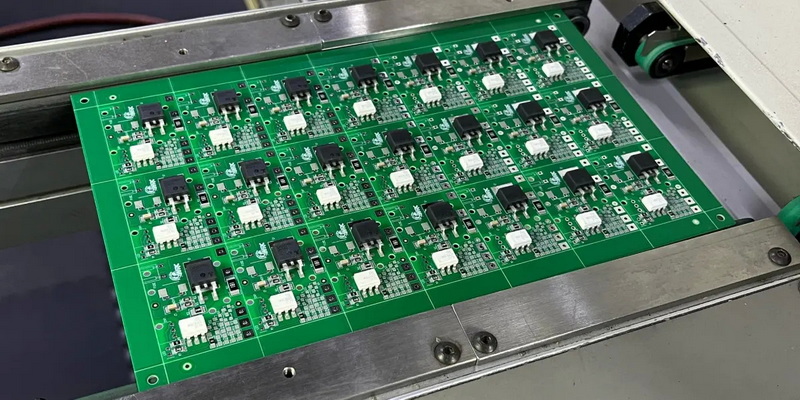
4. Component Placement: After the PCB is fabricated, the components are placed on the board. In SMT, this is typically done using automated pick-and-place machines that accurately position components on the PCB.
5. Soldering: The final step in the SMT prototyping process is soldering the components to the PCB. This can be done using reflow soldering, where the entire board is heated to melt solder paste, or wave soldering for through-hole components.
Advantages of SMT Prototyping
SMT prototyping offers numerous advantages over traditional PCB prototyping methods. Here are some of the key benefits:
1. Compact Design
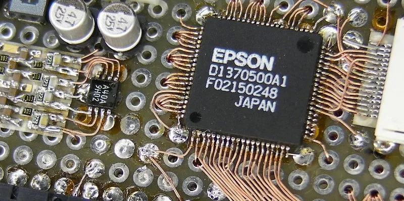
One of the most significant advantages of SMT is the ability to create compact designs. SMT components are generally smaller than their through-hole counterparts, allowing for more components to be placed on a single PCB. This is particularly important in today's electronics market, where space is often at a premium.
2. Improved Performance
SMT components typically have shorter leads, which reduces the distance between the component and the PCB. This leads to lower inductance and capacitance, resulting in improved electrical performance. Additionally, SMT allows for better heat dissipation, which is crucial for high-performance applications.
3. Higher Production Efficiency
The automated processes involved in SMT prototyping lead to higher production efficiency. Automated pick-and-place machines can place thousands of components per hour, significantly reducing the time required to assemble a PCB. This efficiency is particularly beneficial for companies looking to bring products to market quickly.
4. Cost-Effectiveness
While the initial setup costs for SMT prototyping may be higher due to the need for specialized equipment, the overall cost per unit decreases with higher production volumes. The reduced assembly time and lower material costs associated with SMT components contribute to the cost-effectiveness of this method.
5. Enhanced Reliability
SMT components are generally more reliable than through-hole components due to their lower profile and better solder joints. The soldering process used in SMT, such as reflow soldering, creates strong connections that can withstand thermal and mechanical stress.

Applications of SMT Prototyping
SMT prototyping is widely used across various industries, including:
Consumer Electronics
In the consumer electronics sector, SMT prototyping is essential for creating compact and efficient devices such as smartphones, tablets, and wearable technology. The demand for smaller and more powerful devices drives the need for advanced PCB designs.
Automotive Industry
The automotive industry has increasingly adopted SMT prototyping for electronic control units (ECUs), sensors, and infotainment systems. The reliability and performance of SMT components are critical in automotive applications, where safety and efficiency are paramount.
Medical Devices
In the medical field, SMT prototyping is used to develop devices such as diagnostic equipment, monitoring systems, and implantable devices. The compact size and reliability of SMT components are crucial for ensuring the effectiveness and safety of medical devices.
Industrial Automation
SMT prototyping plays a significant role in industrial automation, where PCBs are used in control systems, robotics, and machinery. The ability to create high-density, reliable PCBs is essential for the performance of automated systems.
Challenges in SMT Prototyping
While SMT prototyping offers many advantages, it also presents certain challenges that engineers must address:
1. Design Complexity
The compact nature of SMT components can lead to complex designs that require careful planning and consideration. Engineers must ensure that there is adequate spacing between components to prevent issues such as solder bridging.
2. Thermal Management
As components become smaller and more densely packed, managing heat becomes increasingly important. Engineers must design PCBs with proper thermal management techniques to prevent overheating and ensure reliable operation.
3. Component Availability
Not all components are available in SMT packages, which can limit design options. Engineers must carefully select components that meet their design requirements while also being available in SMT formats.
4. Testing and Debugging
Testing and debugging SMT prototypes can be more challenging than traditional PCBs due to the smaller size and density of components. Engineers must employ specialized testing methods to ensure the functionality of the prototype.
Conclusion
In conclusion, SMT prototyping is a powerful method for PCB design that offers numerous advantages, including compact design, improved performance, higher production efficiency, cost-effectiveness, and enhanced reliability. As technology continues to advance, the demand for high-quality, efficient PCBs will only increase, making SMT prototyping an essential choice for engineers and manufacturers. By understanding the benefits and challenges of SMT prototyping, companies can make informed decisions that lead to successful product development and innovation in the electronics industry.

FAQ
1. What is the main difference between SMT and through-hole technology?
The main difference is that SMT components are mounted directly on the surface of the PCB, while through-hole components are inserted into holes and soldered on the opposite side. SMT allows for more compact designs and improved performance.
2. Why is SMT prototyping preferred for high-volume production?
SMT prototyping is preferred for high-volume production due to its higher production efficiency and lower cost per unit. Automated processes significantly reduce assembly time, making it ideal for mass production.
3. What industries benefit the most from SMT prototyping?
Industries such as consumer electronics, automotive, medical devices, and industrial automation benefit the most from SMT prototyping due to the need for compact, reliable, and high-performance PCBs.
4. What are the challenges associated with SMT prototyping?
Challenges include design complexity, thermal management, component availability, and testing and debugging. Engineers must address these challenges to ensure successful SMT prototyping.
5. How can I ensure the reliability of SMT prototypes?
To ensure reliability, engineers should focus on proper design practices, thermal management, and thorough testing. Using high-quality components and following best practices in soldering can also enhance reliability.


