Content Menu
● Understanding Surface Mount Technology
>> The Evolution of PCB Assembly
● Advantages of SMT in PCB Assembly
>> Miniaturization and Space Efficiency
>> Enhanced Design Flexibility
>> Cost-Effective Production
>> Streamlined Manufacturing Process
>> Improved Electrical Performance
● The SMT Assembly Process
>> 1. PCB Design and Preparation
>> 2. Solder Paste Application
>> 3. Component Placement
>> 4. Reflow Soldering
>> 5. Inspection and Testing
● Challenges and Considerations in SMT Assembly
>> 1. Initial Investment
>> 2. Component Size and Handling
>> 3. Thermal Management
>> 4. Solder Joint Reliability
● SMT vs. Through-Hole Technology
● The Future of SMT in PCB Assembly
>> 1. Increased Miniaturization
>> 2. Integration with Advanced Technologies
>> 3. Improved Automation and AI
>> 4. Sustainability Focus
● Conclusion
● FAQ
>> 1. What is the main difference between SMT and through-hole technology?
>> 2. How does SMT contribute to the miniaturization of electronic devices?
>> 3. Is SMT suitable for all types of electronic products?
>> 4. What are the key challenges in implementing SMT assembly?
>> 5. How is the electronics industry addressing the environmental concerns related to SMT?
● Citations:
In the ever-evolving world of electronics manufacturing, Surface Mount Technology (SMT) has emerged as a game-changer for Printed Circuit Board (PCB) assembly. This innovative approach has revolutionized the way electronic components are mounted on PCBs, offering numerous advantages over traditional through-hole technology. In this comprehensive article, we will explore the reasons why SMT has become the preferred choice for PCB assembly processes, its benefits, challenges, and its impact on the electronics industry.

Understanding Surface Mount Technology
Surface Mount Technology is a method of producing electronic circuits where components are mounted directly onto the surface of printed circuit boards (PCBs). Unlike through-hole technology, which requires components to be inserted through holes in the board, SMT allows for components to be soldered onto pads on the PCB surface[1].
The Evolution of PCB Assembly
The transition from through-hole technology to SMT marks a significant milestone in the history of electronics manufacturing. This shift has been driven by the increasing demand for smaller, lighter, and more complex electronic devices. SMT has enabled manufacturers to meet these demands by allowing for higher component density and more efficient production processes[1].
Advantages of SMT in PCB Assembly
Miniaturization and Space Efficiency
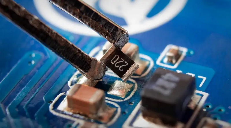
One of the most significant advantages of SMT is its ability to create ultra-thin and miniature PCBs. Surface-mount components are significantly smaller and lighter than their through-hole counterparts, allowing for better utilization of space on printed circuit boards. This compactness enables the design of more compact products without compromising functionality or performance[3].
Enhanced Design Flexibility
SMT provides great flexibility in terms of PCB materials and designs. It enables the use of flexible PCBs (flex PCBs) and rigid-flex PCBs that can bend or conform to specific shapes or spaces. This flexibility opens up opportunities for innovative designs while maintaining excellent electrical performance[3].
Cost-Effective Production
SMT assembly often results in lower production costs, especially for medium to high-volume production runs. The reduced need for drilling holes and the ability to automate the assembly process contribute to cost savings. Additionally, the smaller size of SMT components leads to reduced material costs[3].
Streamlined Manufacturing Process
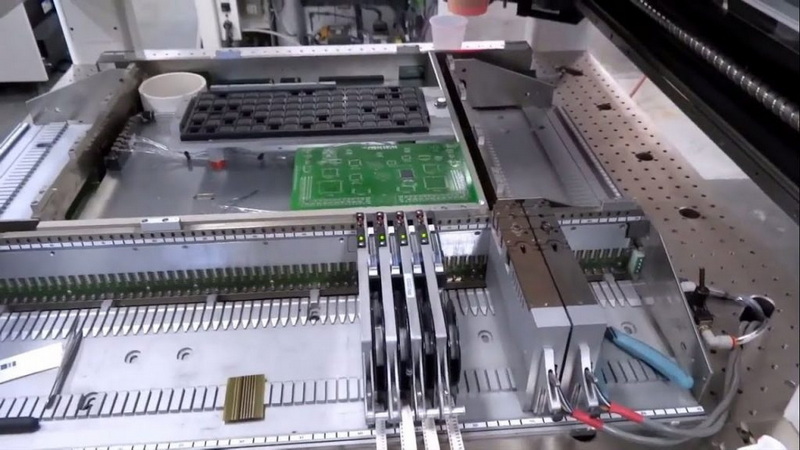
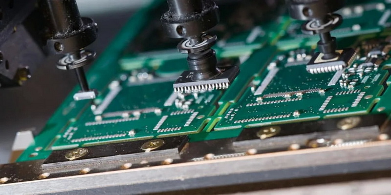
The SMT assembly process is highly amenable to automation, utilizing specialized pick-and-place machines and soldering equipment. This automation reduces reliance on manual labor, decreases assembly time, and minimizes human errors. The simplified manufacturing process leads to increased efficiency and higher production yields[1].
Improved Electrical Performance
SMT components are compatible with high-density double-sided and multi-layer PCB assemblies. This compatibility allows for fast signal transmission with reduced radio frequency interference. The absence of leads in SMT assemblies also improves their resilience to vibration and ensures reliable signal integrity[3].
The SMT Assembly Process
Understanding the SMT assembly process is crucial for appreciating its advantages. Let's break down the key steps involved:
1. PCB Design and Preparation
The process begins with the design of the PCB layout, optimized for SMT components. This step involves careful consideration of component placement, trace routing, and pad design[4].
2. Solder Paste Application
A thin layer of solder paste is applied to the PCB using a stencil. This paste, consisting of tiny solder balls suspended in flux, is crucial for creating reliable solder joints[4].
3. Component Placement
Automated pick-and-place machines precisely position SMT components onto the PCB. These machines can place thousands of components per hour with high accuracy[4].
4. Reflow Soldering
The PCB with placed components passes through a reflow oven. The heat melts the solder paste, creating permanent connections between the components and the PCB[4].
5. Inspection and Testing
After assembly, the PCBs undergo visual and electrical testing to ensure quality and functionality[4].

Challenges and Considerations in SMT Assembly
While SMT offers numerous advantages, it also presents some challenges that manufacturers need to address:
1. Initial Investment
Implementing SMT assembly requires significant initial investment in specialized equipment, such as pick-and-place machines and reflow ovens[1].
2. Component Size and Handling
The small size of SMT components can make manual handling and rework challenging, requiring specialized tools and skilled technicians[1].
3. Thermal Management
The compact nature of SMT assemblies can lead to heat dissipation issues, requiring careful thermal management strategies[1].
4. Solder Joint Reliability
Ensuring reliable solder joints for SMT components, especially in harsh environments, requires precise control of the soldering process and appropriate material selection[1].
SMT vs. Through-Hole Technology
To fully appreciate the benefits of SMT, it's helpful to compare it with traditional through-hole technology:
| Aspect | SMT | Through-Hole |
| Component Size | Smaller | Larger |
| Board Size | Compact | Bulkier |
| Assembly Speed | Faster | Slower |
| Automation | Highly automated | More manual |
| Component Density | Higher | Lower |
| Electrical Performance | Better for high-frequency | Good for high-power |
| Rework | More challenging | Easier |
The Future of SMT in PCB Assembly
As technology continues to advance, SMT is expected to evolve further:
1. Increased Miniaturization
The trend towards smaller and more powerful devices will drive the development of even smaller SMT components and more densely packed PCBs[1].
2. Integration with Advanced Technologies
SMT is likely to be integrated with other advanced manufacturing technologies, such as 3D printing and flexible electronics, opening up new possibilities in product design[1].
3. Improved Automation and AI
The incorporation of artificial intelligence and machine learning is expected to enhance the automation capabilities of SMT assembly processes, leading to even higher efficiency and quality[1].
4. Sustainability Focus
As environmental concerns grow, the SMT industry is likely to focus more on sustainable practices, including the use of lead-free solders and recyclable materials[1].
Conclusion
Surface Mount Technology has undoubtedly revolutionized the PCB assembly process, offering numerous advantages in terms of miniaturization, cost-effectiveness, and production efficiency. While it presents some challenges, the benefits of SMT far outweigh its drawbacks for most modern electronic applications. As technology continues to evolve, SMT is expected to remain at the forefront of PCB assembly techniques, driving innovation in the electronics industry.
The choice of SMT for your PCB assembly process can lead to more compact, efficient, and cost-effective electronic products. By understanding the advantages and considerations of SMT, manufacturers can make informed decisions to optimize their production processes and stay competitive in the rapidly evolving electronics market.

FAQ
1. What is the main difference between SMT and through-hole technology?
SMT involves mounting components directly onto the surface of the PCB, while through-hole technology requires components to be inserted through holes in the board. SMT allows for smaller components, higher density, and more efficient assembly processes[1].
2. How does SMT contribute to the miniaturization of electronic devices?
SMT uses smaller components and allows for higher component density on PCBs. This enables the creation of more compact and lightweight electronic devices without compromising functionality[3].
3. Is SMT suitable for all types of electronic products?
While SMT is widely used and suitable for most modern electronic products, there are still applications where through-hole technology may be preferred, such as for high-power components or in extreme environments where extra mechanical strength is required[1].
4. What are the key challenges in implementing SMT assembly?
The main challenges include the initial investment in specialized equipment, handling of small components, thermal management in densely packed boards, and ensuring reliable solder joints, especially in harsh environments[1].
5. How is the electronics industry addressing the environmental concerns related to SMT?
The industry is focusing on developing lead-free solders, using more recyclable materials, and implementing more energy-efficient manufacturing processes. There's also a growing emphasis on designing products for easier disassembly and recycling at the end of their lifecycle[1].
Citations:
[1] https://www.pcbjhy.com/blog/pros-and-cons-of-smt-pcb-assembly/
[2] https://patents.google.com/patent/CN112040669B/zh
[3] https://www.pcbpower.us/blog/unveiling-the-advantages-and-disadvantages-of-surface-mount-technology
[4] https://blogs.sw.siemens.com/valor-dfm-solutions/how-to-optimize-pcb-design-for-the-smt-assembly-process-flow/
[5] https://levisonenterprises.com/5-advantages-to-using-smt/
[6] https://en.wikipedia.org/wiki/Surface_mount
[7] https://www.pcbelec.com/smt-advantages-and-disadvantages.html
[8] https://www.wevolver.com/article/smt-process


