Content Menu
● Introduction to SMD Components
>> Advantages of SMD Components
● Design Considerations for SMD PCBs
>> Component Placement
>> Pad and Trace Design
>> Design for Manufacturability (DFM) and Testability (DFT)
● Prototyping with SMD Components
>> Using Copper-Clad Boards
>> Adapter Boards
● Advanced PCB Assembly Techniques
>> High-Density Interconnects (HDI)
>> Signal Integrity and Thermal Management
● Future Trends in PCB Design
>> Role of AI in PCB Manufacturing
● Challenges and Solutions in SMD PCB Design
>> Thermal Management Challenges
>> Component Compatibility Issues
● Best Practices for SMD PCB Design
● Conclusion
● FAQ
>> 1. What are the primary advantages of using SMD components in PCB design?
>> 2. How does SMT improve manufacturing efficiency?
>> 3. What are some common challenges in prototyping with SMD components?
>> 4. How does SMT enhance signal integrity?
>> 5. What design considerations are crucial for thermal management in SMD PCBs?
● Citations:
In the realm of electronic design and manufacturing, Surface Mount Devices (SMDs) have become a cornerstone for building efficient and compact prototype PCBs. The use of SMD components in Surface Mount Technology (SMT) offers numerous advantages over traditional through-hole components, making them ideal for modern electronic designs. This article will delve into the benefits of using SMD components in prototype PCB design, exploring their advantages, design considerations, and best practices.

Introduction to SMD Components
SMD components are designed to be mounted directly onto the surface of a Printed Circuit Board (PCB), eliminating the need for holes and manual insertion. This technique allows for higher component density, smaller board sizes, and improved manufacturing efficiency. SMDs are available in various forms, including resistors, capacitors, ICs, and more, each optimized for compactness and performance.
Advantages of SMD Components
1. Higher Component Density: SMD components are significantly smaller than their through-hole counterparts, allowing for more components to be placed on a given PCB area. This high-density capability is crucial for miniaturizing electronic devices while maintaining or enhancing functionality.
2. Smaller and Lighter Assemblies: The compact size of SMD components enables the creation of smaller and lighter PCB assemblies. This is particularly beneficial for portable and handheld electronic devices where size and weight are critical factors.
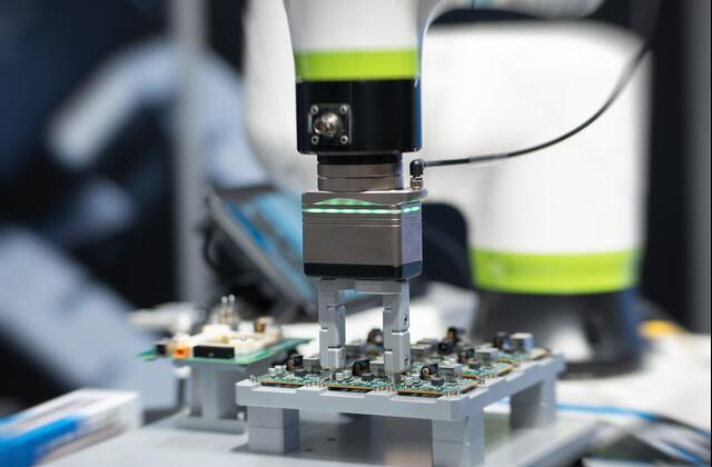
3. Improved Automation Potential: SMT assembly processes are highly amenable to automation, using specialized pick-and-place machines and soldering equipment. This automation reduces assembly time, labor costs, and human errors, making it ideal for high-volume production.
4. Higher Reliability and Longevity: The precision soldering in SMT creates robust interconnections between components and the PCB surface, leading to improved reliability and longer lifespans for SMD assembled PCBs. This is especially advantageous under thermal cycling and vibration stresses.
5. Lower Production Costs at Volume: While the initial investment in SMT equipment may be higher, the efficiency and reliability of automated assembly processes reduce overall production costs for mid to high-volume runs. Additionally, the enhanced reliability minimizes costly rework and warranty claims.
Design Considerations for SMD PCBs
When designing a prototype PCB with SMD components, several key considerations must be addressed to ensure optimal performance and manufacturability.
Component Placement
- Optimize Component Placement: Components should be placed to minimize trace lengths and reduce crosstalk and noise. Critical components like microcontrollers and power supplies should be positioned first.
- Thermal Management: Heat dissipation is crucial, especially for power-intensive components. The layout should facilitate airflow and heat dissipation to prevent component damage.
Pad and Trace Design
- Trace Width and Pad Size: These should be selected based on the current-carrying capacity of the components. Proper spacing between pads is essential for efficient trace routing.
Design for Manufacturability (DFM) and Testability (DFT)
- DFM: Use standard components and footprints to reduce manufacturing costs. Minimize vias and keep trace widths and spacing within standard values.
- DFT: Include test points and access points for testing and debugging. Modular designs simplify testing and reduce test time.
Prototyping with SMD Components
Prototyping with SMD components requires different techniques compared to through-hole components. Here are some methods and tools used for SMD prototyping:
Using Copper-Clad Boards
Prototyping with SMDs can be done without etched PCBs by using copper-clad boards. This involves cutting narrow slots to create rectangular pads for component placement. It requires basic tools like a rotary handheld grinding tool and an awl.
Adapter Boards
Another method is using adapter boards, which are readily available. SMDs are soldered onto these boards, allowing for quick testing and prototyping of low-power devices.

Advanced PCB Assembly Techniques
Recent advancements in PCB assembly have further enhanced the capabilities of SMD components. Techniques such as microvias and fine-pitch component placement allow for more complex and compact designs. Microvias enable precise interconnection between layers, while fine-pitch components require high-precision placement equipment to prevent misalignment or solder bridging[7].
High-Density Interconnects (HDI)
HDI technology has revolutionized PCB design by allowing for an unprecedented number of components to be integrated into smaller spaces. This is achieved through advanced layer densities and the seamless integration of microvias, which optimize signal paths and maximize PCB real estate[2].
Signal Integrity and Thermal Management
Maintaining signal integrity and managing thermal issues are critical challenges in modern PCB design. Techniques like via-in-pad and controlled impedance routing help reduce signal distortion and improve thermal management. Via-in-pad technology allows for higher routing densities, reducing signal degradation and enhancing overall performance[2][6].
Future Trends in PCB Design
The future of PCB design is shaped by trends such as miniaturization, automation, and sustainability. As devices become smaller and more powerful, the demand for high-density interconnects and advanced SMT methods increases. AI-driven manufacturing processes are transforming PCB assembly by optimizing workflows, reducing waste, and improving quality control[5].
Role of AI in PCB Manufacturing
AI is increasingly being integrated into PCB manufacturing to enhance efficiency and accuracy. AI-powered automated optical inspection (AOI) and robotic soldering are becoming essential tools for modern PCB assembly, enabling faster production with fewer errors[5].
Challenges and Solutions in SMD PCB Design
Despite the advantages of SMD components, several challenges arise during design and assembly. These include thermal management, component compatibility, and signal integrity.
Thermal Management Challenges
As devices become more compact, thermal management becomes a significant concern. SMD components generate heat, which can affect performance and longevity if not managed properly. Solutions include using components with built-in thermal pads or heatsinks, improving PCB layout for better airflow, and employing advanced cooling methods like forced air or liquid cooling for high-power applications[3].
Component Compatibility Issues
Ensuring component compatibility is crucial for optimal performance. Different components have varying package types, pin configurations, and sizes, which can complicate assembly and impact circuit performance. Designers should select components that meet specific application requirements and use simulation tools to identify potential compatibility issues early in the design phase[3].
Best Practices for SMD PCB Design
To ensure efficient and reliable SMD PCB designs, consider the following best practices:
- Flexibility in Design: SMT allows for flexible PCB designs, including flex PCBs and rigid-flex PCBs, which can conform to specific shapes or spaces.
- Material and Cost Efficiency: SMT reduces material costs by eliminating the need for holes and manual insertion, making it more cost-effective for high-volume production.
- Signal Integrity: SMT components facilitate fast signal transmission with less radio frequency interference, ensuring dependable signal integrity.
Conclusion
Incorporating SMD components into prototype PCB designs offers numerous benefits, from higher component density and automation potential to improved reliability and cost efficiency. By understanding the advantages and design considerations of SMD components, engineers can create more efficient, compact, and reliable electronic devices. Whether for prototyping or mass production, SMD components are a crucial choice for modern electronic design.

FAQ
1. What are the primary advantages of using SMD components in PCB design?
SMD components offer higher component density, smaller and lighter assemblies, improved automation potential, higher reliability, and lower production costs at volume compared to through-hole components.
2. How does SMT improve manufacturing efficiency?
SMT improves manufacturing efficiency by allowing for automated assembly processes using pick-and-place machines and reflow soldering, reducing labor costs and human errors.
3. What are some common challenges in prototyping with SMD components?
Common challenges include handling small components, requiring specialized tools for manual assembly, and the need for precise component placement to avoid errors.
4. How does SMT enhance signal integrity?
SMT enhances signal integrity by reducing radio frequency interference due to the lack of leads in SMD components, ensuring fast and reliable signal transmission.
5. What design considerations are crucial for thermal management in SMD PCBs?
Thermal management in SMD PCBs involves optimizing component placement to facilitate airflow and heat dissipation, especially for power-intensive components.
Citations:
[1] https://jlcpcb.com/blog/design-process-of-a-surface-mount-pcb
[2] https://www.911eda.com/news/pcb-design-trends-in-2024/
[3] https://www.x-pcb.com/challenges-of-smd-overcoming-the-obstacles-in-modern-electronics/
[4] https://morepcb.com/smd-assembly-a-comprehensive-guide/
[5] https://novaenginc.com/future-of-circuit-board-assembly/
[6] https://www.electronicdesign.com/technologies/eda/printed-circuit-boards/article/55041417/viasion-technology-top-5-miniaturization-challenges-in-pcb-assembly-and-their-solutions
[7] https://www.rigiflex.com/blog/get-to-know-about-the-advanced-pcb-assembly-techniques-for-complex-circuits/
[8] https://swimbi.com/smd-pcb-layout-tips-and-best-practices-for-efficient-design/
[9] https://www.protoexpress.com/blog/pcb-design-challenges-with-solutions-for-engineers/
[10] https://electronics.stackexchange.com/questions/174082/making-prototypes-with-high-speed-smd-components
[11] https://www.rs-online.com/designspark/latest-pcb-technology-and-industry-trends
[12] https://jlcpcb.com/blog/common-problems-and-solutions-in-PCB-design
[13] https://bayareacircuits.com/exploring-advanced-pcb-design-techniques-for-enhanced-performance/
[14] https://www.zuken.com/en/blog/the-top-pcb-design-trends-to-watch-in-2025/
[15] https://resources.altium.com/p/solving-modern-pcb-layout-challenges
[16] https://www.eevblog.com/forum/projects/smd-prototyping-techniques/
[17] https://highpcb.com/top-5-emerging-trends-in-pcb-technology-for-2025/
[18] https://www.pcbcart.com/article/content/the-most-common-problems-in-pcb-design.html
[19] https://www.reddit.com/r/AskElectronics/comments/4hqfht/smd_prototyping_methods/
[20] https://www.eevblog.com/forum/beginners/tht-versions-of-smd-components/


