Content Menu
● Understanding SMT Stencils and Their Role
>> Types of SMT Stencils
>> Materials and Manufacturing
● Why Makers Are Choosing SMT Stencil Self-Production
>> 1. Cost Efficiency
>> 2. Faster Turnaround and Flexibility
>> 3. Accessibility of Tools and Resources
>> 4. Skill Development and Learning
>> 5. Customization and Experimentation
● How SMT Stencils Improve PCB Assembly
● How to Make SMT Stencils Yourself
>> Materials Needed
>> Step-by-Step DIY SMT Stencil Production
>> Tips for Better Results
● Common Problems and Solutions in DIY SMT Stencil Use
>> Solder Paste Release Issues
>> Solder Bridges and Shorts
>> Poor Print Quality or Incomplete Fills
● Benefits of SMT Stencil Self-Production for Makers
● Challenges and Considerations
● Conclusion
● FAQ
>> 1. What materials can I use to make SMT stencils myself?
>> 2. What equipment do I need to create my own SMT stencil?
>> 3. How do I ensure my DIY stencil aligns correctly with the PCB?
>> 4. Can DIY SMT stencils be used for high-volume production?
>> 5. What are common problems when making SMT stencils myself?
Surface Mount Technology (SMT) has revolutionized electronics manufacturing by enabling the production of compact, high-performance printed circuit boards (PCBs). At the heart of this process lies the SMT stencil-a precision tool that applies solder paste accurately onto PCB pads. Recently, a growing number of makers and small-scale manufacturers are choosing to create SMT stencils themselves instead of relying on external suppliers. This article explores the reasons behind this trend, the benefits and challenges of SMT stencil self-production, and practical guidance on how to make your own stencils.

Understanding SMT Stencils and Their Role
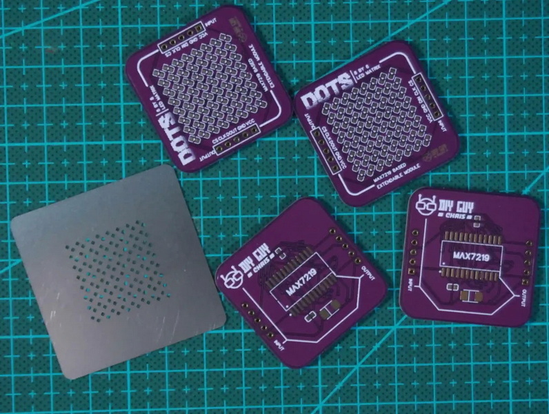
An SMT stencil is a thin metal sheet, typically stainless steel or nickel alloy, with laser-cut apertures that correspond exactly to the solder pads on a PCB. These apertures allow solder paste to be deposited precisely where components will be mounted, ensuring reliable solder joints and overall product quality.
Types of SMT Stencils
- Framed Stencils: Mounted in rigid frames, ideal for high-volume production due to their stability and accuracy.
- Frameless Stencils: Flexible foil stencils used mainly for prototyping and small runs, easily stored and adaptable.
- Step Stencils: Feature multiple thickness levels to optimize solder paste volume for components with varying pad sizes.
Materials and Manufacturing
Stainless steel is the most common material for durable stencils, while nickel alloys offer high-temperature resistance. Laser cutting is the preferred manufacturing method, offering high precision necessary for fine-pitch components, with typical hole size errors as low as 0.3–0.5 mil and positioning accuracy under 0.12 mil. Chemical etching is a less precise but cost-effective alternative.
Why Makers Are Choosing SMT Stencil Self-Production
1. Cost Efficiency
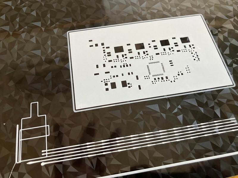
Commercial SMT stencils, especially for small runs or prototypes, can be surprisingly expensive-sometimes costing more than the PCBs themselves. Makers can significantly reduce costs by producing stencils in-house using affordable materials like kapton or mylar films and accessible tools such as laser cutters.
2. Faster Turnaround and Flexibility
Ordering stencils from external vendors involves lead times that can delay project schedules. Self-production allows makers to rapidly iterate designs, test new PCB layouts, and adapt to changes without waiting for external fabrication.
3. Accessibility of Tools and Resources
The availability of affordable laser cutters and open-source PCB design software has democratized stencil making. Makers can export solder paste layers from software like EagleCAD or KiCAD and create precise stencil designs, then cut these at home or via local makerspaces.
4. Skill Development and Learning
Making SMT stencils themselves deepens makers' understanding of the SMT assembly process, improving their electronics manufacturing skills. This hands-on approach fosters innovation and problem-solving abilities.
5. Customization and Experimentation
Self-made stencils enable experimentation with custom aperture shapes, step stencils, and various thicknesses to optimize solder paste deposition for unique or complex PCB designs, which might be cost-prohibitive or unavailable from commercial suppliers.
How SMT Stencils Improve PCB Assembly
Using SMT stencils solves many problems faced in manual PCB assembly:
- No Short Circuits: Precise solder paste application reduces bridging risks.
- No Gaps in Soldering: Laser-cut stencils allow smooth, even paste layers with no gaps.
- Smooth Pad Walls: Stencils ensure consistent solder paste shapes, improving joint quality.
- Consistent Aperture Quality: High-precision laser cutting produces accurate apertures with trapezoidal walls for optimal paste release.
- Increased Efficiency: Stencils enable simultaneous paste application to all pads, speeding up assembly.
- Compatibility with Automation: Essential for solder paste printers in automated assembly lines.

How to Make SMT Stencils Yourself
Materials Needed
- Kapton or mylar film (commonly 2 mil thickness) or thin stainless steel sheets for higher durability
- Access to a laser cutter or local makerspace with laser cutting services
- PCB design software to export solder paste layers (e.g., EagleCAD, KiCAD)
- Gerber viewer for stencil design verification
- Squeegee or plastic card for applying solder paste
- Double-sided adhesive tape for stencil alignment
- Isopropyl alcohol and nitrile gloves for cleaning
Step-by-Step DIY SMT Stencil Production
1. Design Preparation: Export the solder paste layer from your PCB design software in Gerber format, including PCB outline and fiducials for alignment.
2. Stencil Material Setup: Choose appropriate stencil material-kapton/mylar for prototyping or stainless steel for durability. Clean and prepare sheets by removing oils and dust.
3. Laser Cutting: Use optimized laser settings to cut apertures cleanly without melting the material. Test cuts on scrap material help dial in parameters. Ensure tapered aperture walls (~80 degrees) for clean paste release.
4. Stencil Alignment: Use fiducial marks on both stencil and PCB to ensure precise placement during solder paste application. Tape the stencil to the PCB with a hinge tape method for repeatable alignment.
5. Solder Paste Application: Apply solder paste through the stencil using a squeegee or plastic card. Apply even pressure across the stencil surface to achieve uniform paste deposition.
6. Cleaning and Maintenance: After use, clean the stencil with isopropyl alcohol to remove residual paste and prevent clogging. Store stencils in anti-static paper to avoid dust accumulation.
Tips for Better Results
- Use nano-coatings or electropolishing on metal stencils to improve solder paste release.
- Create a hinge with tape on DIY stencils for easy lifting and repositioning during paste application.
- Experiment with stencil thickness (typically 0.1–0.15 mm) to balance paste volume and print quality.
- Maintain cleanliness of stencil, PCB, and work area to prevent printing defects.
Common Problems and Solutions in DIY SMT Stencil Use
Solder Paste Release Issues
- Misalignment between stencil apertures and PCB pads causes insufficient or inconsistent paste deposits.
- Dried paste or oils blocking apertures can reduce paste flow.
- Inadequate stencil anchoring during printing leads to smearing or uneven deposits.
Solution: Ensure precise alignment, clean stencil regularly, and apply consistent pressure during paste application.
Solder Bridges and Shorts
- Excessive paste volume or poor squeegee technique can cause solder bridging between pads.
- Paste drying inside apertures or misalignment increases bridging risk.
Solution: Optimize paste volume, squeegee angle, and stencil cleaning.
Poor Print Quality or Incomplete Fills
- Aperture size mismatch or rounded corners reduce print definition.
- Insufficient clamping or movement during printing causes smearing.
Solution: Match apertures precisely to pad sizes, use proper stencil clamping, and maintain cleanliness.
Benefits of SMT Stencil Self-Production for Makers
- Cost Savings: Avoid high prices of commercial stencils, especially for prototypes and small batches.
- Speed: Immediate stencil availability accelerates prototyping cycles.
- Customization: Tailor stencil design to specific project needs, including step stencils and unique apertures.
- Skill Enhancement: Hands-on experience with SMT assembly improves manufacturing expertise.
- Sustainability: Produce only what is needed, reducing waste.
Challenges and Considerations
- Precision Requirements: Achieving high-quality stencils requires precise laser cutting and careful design.
- Material Limitations: DIY stencil materials like kapton are less durable than stainless steel.
- Learning Curve: Makers must invest time to master design, cutting, and printing techniques.
- Equipment Access: Not all makers have easy access to laser cutters or clean workspaces.
Conclusion
The growing trend of makers creating SMT stencils themselves is driven by cost savings, faster iteration cycles, accessible tools, and the desire for customization. While challenges exist, the benefits for prototyping and small-scale production are significant. As laser cutting technology and DIY resources improve, SMT stencil self-production will become even more widespread, empowering makers to innovate and produce electronics with greater independence and efficiency.

FAQ
1. What materials can I use to make SMT stencils myself?
You can use kapton or mylar films for DIY stencils, which are affordable and laser-cuttable. For professional-grade stencils, stainless steel sheets offer greater durability and precision.
2. What equipment do I need to create my own SMT stencil?
A laser cutter is essential for precise aperture cutting. Additionally, PCB design software to export solder paste layers and a Gerber viewer help prepare the stencil design.
3. How do I ensure my DIY stencil aligns correctly with the PCB?
Use fiducial marks on both stencil and PCB for accurate alignment. Employ hinge tape methods to fix the stencil in place during solder paste application.
4. Can DIY SMT stencils be used for high-volume production?
DIY stencils are best suited for prototyping and small batch runs. For high-volume manufacturing, framed stainless steel stencils provide better durability and consistency.
5. What are common problems when making SMT stencils myself?
Common issues include melted stencil material due to improper laser settings, poor aperture quality, misalignment during printing, and solder bridging. Proper thermal management, cleaning, and alignment techniques mitigate these problems.


