Content Menu
● Understanding SMT and DIP Technologies
>> Surface Mount Technology (SMT)
>> Dual In-line Package (DIP) Technology
● Comparing SMT and DIP: Key Factors
>> Size and Space Efficiency
>> Assembly Process and Automation
>> Reliability and Mechanical Strength
>> Electrical Performance
>> Rework and Repair
● Cost Considerations
>> Component Costs
>> Assembly Costs
>> Overall Production Costs
● Applications and Industry Preferences
>> Consumer Electronics
>> Automotive Electronics
>> Aerospace and Military
>> Industrial Equipment
● Future Trends in PCB Assembly
>> Miniaturization
>> Mixed Technology
>> Advanced Materials
>> Automation and Industry 4.0
● Environmental Considerations
>> Material Usage
>> Energy Consumption
>> Recyclability
● Making the Choice: SMT or DIP?
● Conclusion
● FAQ
>> 1. What are the main differences between SMT and DIP in PCB assembly?
>> 2. How does SMT impact the miniaturization of electronic devices?
>> 3. Is DIP technology becoming obsolete in PCB assembly?
>> 4. How do SMT and DIP compare in terms of cost-effectiveness?
>> 5. What are the environmental implications of choosing SMT over DIP?
● Citations:
In the world of electronic manufacturing, printed circuit board (PCB) assembly is a critical process that determines the functionality, reliability, and efficiency of electronic devices. Two primary technologies dominate this field: Surface Mount Technology (SMT) and Dual In-line Package (DIP) technology, also known as Through-Hole Technology (THT). Both methods have their unique characteristics, advantages, and drawbacks, making the choice between them a crucial decision for manufacturers and engineers alike.

Understanding SMT and DIP Technologies
Surface Mount Technology (SMT)
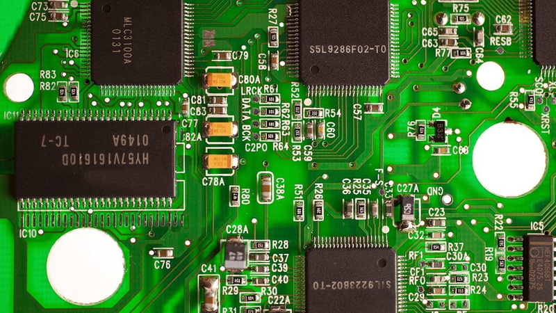
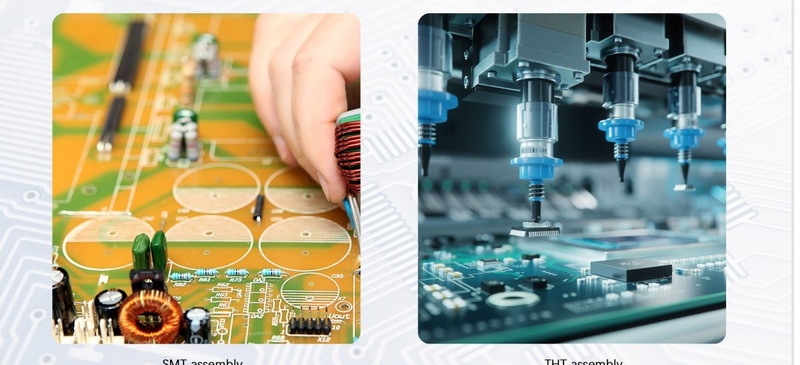
Surface Mount Technology is a method of PCB assembly where components are mounted directly onto the surface of the board[1]. This technology has revolutionized the electronics industry since its widespread adoption in the 1980s. SMT components, known as Surface Mount Devices (SMDs), are typically smaller and have short leads or no leads at all.
Dual In-line Package (DIP) Technology
DIP technology, also referred to as Through-Hole Technology, involves components with leads that are inserted through holes drilled in the PCB and soldered on the opposite side[5]. This method has been in use since the early days of electronic manufacturing and continues to be relevant for certain applications.
Comparing SMT and DIP: Key Factors
Size and Space Efficiency
SMT has a clear advantage when it comes to size and space efficiency. SMT components are significantly smaller than their DIP counterparts, allowing for more compact PCB designs[2]. This miniaturization capability has been crucial in the development of smaller, lighter electronic devices such as smartphones, wearables, and IoT devices[7].
DIP components, on the other hand, require more board space due to their larger size and the need for drilled holes. This can limit the overall density of components on a PCB and result in larger end products[3].
Assembly Process and Automation
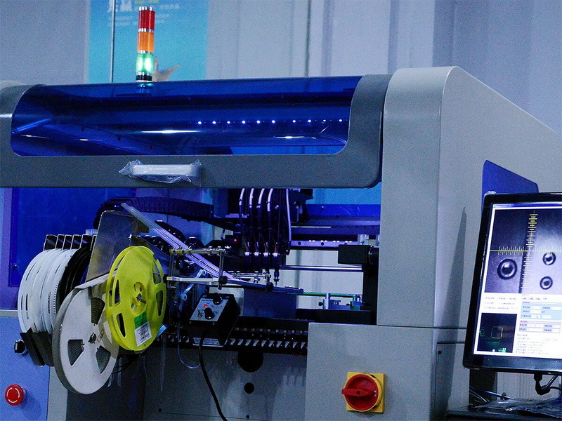
SMT assembly is highly automated, utilizing advanced machinery such as pick-and-place machines and reflow ovens. This automation leads to faster production times and higher efficiency[2]. The SMT process typically involves:
1. Applying solder paste to the PCB
2. Placing components using SMT machines
3. Reflow soldering to secure components
DIP assembly, while it can be automated to some extent, often requires more manual intervention, especially for complex boards. The process usually involves:
1. Inserting components into pre-drilled holes
2. Wave soldering or manual soldering to secure components
The higher level of automation in SMT results in faster production rates and lower labor costs, making it more suitable for high-volume production[3].
Reliability and Mechanical Strength
DIP technology has long been praised for its mechanical strength and reliability. The through-hole design provides a stronger physical connection between the component and the PCB, making DIP assemblies more resistant to mechanical stress, vibration, and thermal cycling[3].
SMT, while generally reliable, may be more susceptible to mechanical stresses. However, advancements in SMT techniques and materials have significantly improved its reliability over the years[6].
Electrical Performance
SMT offers superior electrical performance in many aspects. The shorter leads and closer proximity of components to the PCB surface result in reduced parasitic capacitance and inductance. This characteristic makes SMT ideal for high-frequency applications[2].
DIP components, with their longer leads, may introduce more parasitic effects, potentially impacting signal integrity in high-speed circuits. However, for lower frequency applications, this difference may be negligible[3].
Rework and Repair
When it comes to rework and repair, DIP technology has an advantage. Through-hole components are generally easier to replace or repair manually. Technicians can access individual pins and solder joints more easily[6].
SMT components, especially fine-pitch or ball grid array (BGA) packages, can be challenging to rework. Special equipment and skills are often required for SMT rework, which can increase maintenance costs[6].
Cost Considerations
Component Costs
SMT components are generally less expensive than their DIP counterparts due to their smaller size and mass production. The reduced material usage in SMT components contributes to lower costs, especially in high-volume production scenarios[2].
Assembly Costs
While SMT equipment requires a higher initial investment, the increased automation and efficiency lead to lower assembly costs per unit, especially for large production runs. DIP assembly, with its higher labor requirements, can be more cost-effective for small production volumes or prototyping[3].
Overall Production Costs
When considering total production costs, SMT often comes out ahead, particularly for high-volume manufacturing. The combination of cheaper components, faster assembly times, and reduced material usage contributes to lower overall costs[2].

Applications and Industry Preferences
Consumer Electronics
The consumer electronics industry heavily favors SMT due to its ability to produce compact, lightweight devices. Smartphones, tablets, and wearables rely almost exclusively on SMT for their PCB assembly[7].
Automotive Electronics
The automotive sector uses a mix of SMT and DIP technologies. While SMT is preferred for most applications due to its space-saving properties, DIP is still used in areas requiring high reliability and resistance to extreme conditions[3].
Aerospace and Military
Aerospace and military applications often prioritize reliability and durability over size. As a result, DIP technology is still widely used in these sectors, although SMT is gaining ground as its reliability improves[3].
Industrial Equipment
Industrial equipment manufacturers often use a combination of SMT and DIP, depending on the specific requirements of each application. DIP might be preferred for components that need to withstand harsh environments or frequent maintenance[5].
Future Trends in PCB Assembly
Miniaturization
The trend towards smaller, more powerful devices continues to drive the adoption of SMT. As components become even smaller, new challenges in assembly and inspection arise, pushing the boundaries of SMT capabilities[7].
Mixed Technology
Many modern PCBs use a combination of SMT and DIP technologies, known as mixed technology assembly. This approach allows designers to leverage the strengths of both methods, optimizing for performance, reliability, and cost[3].
Advanced Materials
The development of new solder materials and PCB substrates is enhancing the reliability and performance of both SMT and DIP assemblies. These advancements may further blur the lines between the two technologies in terms of reliability and durability[6].
Automation and Industry 4.0
The increasing integration of automation, artificial intelligence, and data analytics in PCB assembly processes is improving efficiency and quality for both SMT and DIP technologies. However, SMT is likely to benefit more from these advancements due to its already high level of automation[7].
Environmental Considerations
Material Usage
SMT generally uses less material than DIP, both in terms of component size and PCB substrate. This reduced material usage can lead to a lower environmental impact[2].
Energy Consumption
The automated nature of SMT assembly often results in more energy-efficient production processes compared to DIP assembly. However, the energy intensity of individual components and their lifecycle energy consumption should also be considered[6].
Recyclability
The recyclability of PCBs assembled with SMT or DIP technologies can vary. While SMT boards may be more compact and use less material, the smaller size of components can make separation and recycling more challenging. DIP components, being larger, may be easier to separate for recycling purposes[6].
Making the Choice: SMT or DIP?
The decision between SMT and DIP technology depends on various factors:
1. Product requirements (size, performance, durability)
2. Production volume
3. Budget constraints
4. Industry standards and regulations
5. Environmental considerations
For most modern applications, especially those requiring miniaturization and high-volume production, SMT is the preferred choice. However, DIP technology still holds its ground in applications where extreme reliability, ease of repair, or compatibility with existing systems is crucial[3].
Conclusion
Both SMT and DIP technologies have their place in modern PCB assembly. SMT offers significant advantages in terms of miniaturization, automation, and cost-effectiveness for high-volume production. It has become the dominant technology in consumer electronics and is making inroads into other sectors.
DIP technology, while less prevalent, still offers unmatched reliability and ease of repair, making it valuable in aerospace, military, and certain industrial applications. The choice between SMT and DIP should be based on a careful analysis of the specific requirements of each project, considering factors such as performance needs, production volume, environmental conditions, and lifecycle considerations.
As technology continues to evolve, we may see further convergence of these technologies or the emergence of new assembly methods that combine the best of both worlds. For now, understanding the strengths and limitations of both SMT and DIP technologies is crucial for making informed decisions in PCB assembly.

FAQ
1. What are the main differences between SMT and DIP in PCB assembly?
SMT (Surface Mount Technology) involves mounting components directly onto the surface of the PCB, while DIP (Dual In-line Package) or Through-Hole Technology requires components to be inserted through holes in the board. SMT allows for smaller, more compact designs and is more suitable for automation, while DIP provides stronger mechanical connections and is easier to repair manually.
2. How does SMT impact the miniaturization of electronic devices?
SMT significantly contributes to the miniaturization of electronic devices by allowing for smaller components and higher component density on PCBs. This technology enables the creation of compact, lightweight devices such as smartphones, wearables, and IoT devices, which would be difficult or impossible to achieve with traditional DIP technology.
3. Is DIP technology becoming obsolete in PCB assembly?
While SMT has become the dominant technology in many areas, DIP is not obsolete. It remains valuable in applications requiring high reliability, ease of repair, or compatibility with existing systems. DIP is still widely used in aerospace, military, and certain industrial applications where durability and resistance to extreme conditions are crucial.
4. How do SMT and DIP compare in terms of cost-effectiveness?
SMT is generally more cost-effective for high-volume production due to its automation capabilities and smaller component sizes. However, DIP can be more cost-effective for small production runs or prototyping due to lower equipment costs and easier manual assembly. The overall cost-effectiveness depends on factors such as production volume, component costs, and specific application requirements.
5. What are the environmental implications of choosing SMT over DIP?
SMT typically uses less material than DIP, both in terms of component size and PCB substrate, potentially leading to a lower environmental impact. SMT assembly processes are often more energy-efficient due to automation. However, the smaller size of SMT components can make recycling more challenging compared to larger DIP components. The overall environmental impact depends on various factors, including lifecycle energy consumption and recyclability of the entire product.
Citations:
[1] https://www.fastturnpcbs.com/differences-in-characteristics-and-applications-between-smt-and-dip/
[2] https://www.candorind.com/blog/surface-mount-vs-through-hole/
[3] https://www.absoluteelectronics.net/comparing-pcb-assembly-methods-pros-and-cons-of-smt-through-hole-and-mixed-technology/
[4] https://www.hongzhousmart.com/pcb-pcba-factory-smt-dip-technology-pcba-assembly-4387.html
[5] https://www.linkedin.com/pulse/what-smt-dip-difference-between-genevieve-li
[6] https://www.pcbelec.com/smt-advantages-and-disadvantages.html
[7] https://www.zetwerk.com/resources/knowledge-base/electronics-manufacturing-services-ems/smt-vs-through-hole-choosing-the-right-pcb-assembly-technique/
[8] https://jxpcba.en.made-in-china.com/product/WErRXeFPOmhQ/China-Electronics-Assembly-SMT-DIP-PCB-PCBA-Protypes.html
[9] https://www.grande-pcba.com/whats-the-difference-between-smt-components-dip-components-used-in-pcb-assembly/
[10] https://rootsems.com/advantages-and-disadvantages-of-surface-mount-technology/
[11] https://www.pcb-hero.com/blogs/lickys-column/tht-vs-smd-which-is-the-better-pcb-assembly-process
[12] https://www.neodensmt.com/news/what-does-smt-pcb-pcba-dip-mean-51532401.html


