Content Menu
● Introduction to SMT PCB Assembly
>> Benefits of SMT
● SMT PCB Assembly Process Step-by-Step
>> 1. PCB Design
>> 2. Stencil Creation
>> 3. Solder Paste Application
>> 4. Component Placement
>> 5. Reflow Soldering
>> 6. Inspection and Testing
>> 7. Conformal Coating
>> 8. Final Assembly
● SMT Assembly Equipment
● Common Defects in SMT Assembly
● Improving SMT Assembly Efficiency
● Future Trends in SMT Assembly
● Conclusion
● FAQs
>> 1. What are the main advantages of SMT vs. through-hole assembly?
>> 2. What types of components are not suitable for SMT?
>> 3. Can SMT boards be repaired?
>> 4. How are very small components handled in SMT?
>> 5. What innovations are occurring in SMT assembly?
Surface Mount Technology (SMT) has transformed the landscape of electronics manufacturing, allowing for the assembly of printed circuit boards (PCBs) with greater efficiency and compactness. This article provides a comprehensive overview of the SMT PCB assembly process, detailing each step involved, the equipment used, and the benefits of this technology.

Introduction to SMT PCB Assembly
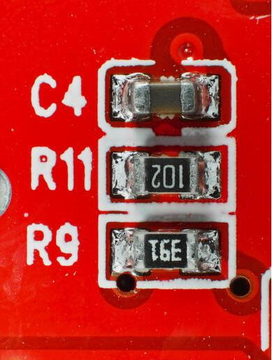
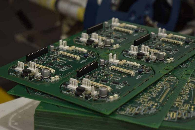
SMT is a method where electronic components are mounted directly onto the surface of PCBs, as opposed to the traditional through-hole technology where components are inserted into drilled holes. This method has several advantages, including reduced size and weight of the boards, higher component density, and improved performance due to shorter electrical paths.
Benefits of SMT
1. Compact Design: SMT components are smaller and can be placed on both sides of the PCB, allowing for more complex and compact designs.
2. Increased Speed and Efficiency: Automated placement and soldering processes lead to faster production times.
3. Enhanced Performance: Shorter lead lengths improve electrical performance and signal integrity.
4. Cost-Effectiveness: Reduced material costs and faster production times contribute to overall savings.
5. Improved Reliability: Fewer mechanical connections enhance durability and reliability.
SMT PCB Assembly Process Step-by-Step
The SMT assembly process consists of several critical steps, each essential for ensuring the proper placement and soldering of components. Below is a detailed breakdown of these steps:
1. PCB Design
The first step involves designing the PCB layout specifically for SMT components. This includes creating pads for the components and ensuring that design rules are met using specialized software. Simulations may also be conducted to test manufacturability. The design phase is crucial as it sets the foundation for the entire assembly process. Engineers must consider factors such as component placement, trace routing, and thermal management to optimize the performance of the final product.
2. Stencil Creation
A metal stencil is created with cutouts that match the PCB pads. This stencil is used for applying solder paste accurately to the PCB. The stencil must be designed with precision to ensure that the right amount of solder paste is deposited on each pad. This step is critical because insufficient solder can lead to weak connections, while excess solder can cause bridging between pads.
3. Solder Paste Application
Solder paste, a mixture of solder particles and flux, is applied to the PCB through the stencil openings. Common methods for this application include screen printing, jet printing, and dispensing. Screen printing is the most widely used method due to its speed and efficiency. The application of solder paste must be uniform to ensure consistent solder joints during the reflow process.
4. Component Placement
SMT components are placed onto the solder paste deposits using high-speed pick-and-place machines. These machines can handle components from reels, trays, or sticks, ensuring precise placement. The accuracy of this step is vital, as misalignment can lead to soldering defects. Advanced pick-and-place machines are equipped with vision systems that allow them to verify the position of components before soldering, further enhancing placement accuracy.
5. Reflow Soldering
The PCB is then passed through a reflow oven, where the solder paste melts and joins the components to the pads. The reflow process typically includes several temperature zones: ramp-up, reflow, and cool-down. Each zone is carefully controlled to ensure that the solder paste reaches the appropriate temperature for melting and then cools down at a controlled rate to form strong solder joints. The reflow oven can be either convection or infrared, with convection being the most common due to its uniform heating capabilities.
6. Inspection and Testing
After soldering, the PCB undergoes inspection to check for assembly defects. This can involve automated optical inspection (AOI) and electrical testing to ensure proper functionality. AOI systems use high-resolution cameras to detect issues such as misaligned components, insufficient solder, and solder bridges. Electrical testing, including in-circuit testing (ICT) and functional testing, verifies that the assembled PCB operates as intended.
7. Conformal Coating
A protective coating may be applied to the PCB to prevent environmental damage. This can be done through various methods, including spraying, dipping, or vapor deposition. Conformal coatings protect against moisture, dust, chemicals, and temperature extremes, which can significantly enhance the reliability and lifespan of electronic devices.
8. Final Assembly
In the final step, additional components may be attached, and the PCB is prepared for integration into the final product. This may involve adding connectors, heat sinks, or other mechanical components. The final assembly stage is crucial for ensuring that the PCB fits correctly within the overall product design and functions as intended.

SMT Assembly Equipment
The SMT assembly process requires specialized equipment at each stage:
| Equipment Type | Description |
| Solder Paste Printers | Use screens or stencils to apply solder paste. |
| Pick and Place Machines | Automated machines that place components onto the PCB. |
| Reflow Ovens | Heat the PCB to melt solder and form connections. |
| Inspection Systems | Automated systems for quality control, including AOI and X-ray inspection. |
| Conformal Coating Equipment | Apply protective coatings to PCBs. |
Common Defects in SMT Assembly
Despite the efficiency of SMT, defects can occur. Common issues include:
- Soldering Defects: Insufficient solder, solder bridges, and tombstoning. Insufficient solder can lead to weak connections, while solder bridges can cause short circuits. Tombstoning occurs when one end of a component lifts off the PCB during soldering, resulting in a poor connection.
- Part Placement Defects: Misalignments and incorrect components. Misalignment can lead to soldering issues, while using the wrong component can result in functional failures.
- Physical Damage: Cracks or warping due to mishandling. Physical damage can occur during transport or handling, affecting the integrity of the PCB.
Improving SMT Assembly Efficiency
To enhance the efficiency of the SMT assembly process, manufacturers can:
- Design for Manufacturability (DFM): Create PCB layouts that are optimized for assembly. DFM principles help reduce complexity and improve yield.
- Utilize Libraries: Use manufacturer component libraries to streamline design. Libraries provide standardized component footprints, reducing design time and errors.
- Standardize Designs: Reuse proven designs to reduce complexity. Standardization can lead to faster production times and lower costs.
- Automate Inspection: Implement automated testing to catch defects early. Early detection of defects can save time and resources in the production process.
Future Trends in SMT Assembly
As technology continues to evolve, several trends are shaping the future of SMT assembly:
1. Miniaturization: The demand for smaller and more compact electronic devices is driving the development of even smaller SMT components. This trend requires advanced placement techniques and equipment capable of handling micro-components.
2. Smart Manufacturing: The integration of IoT and AI in manufacturing processes is enhancing efficiency and quality control. Smart factories can monitor production in real-time, allowing for immediate adjustments to improve yield and reduce waste.
3. Sustainability: There is a growing emphasis on environmentally friendly practices in electronics manufacturing. This includes the use of lead-free solder, recyclable materials, and energy-efficient processes.
4. Advanced Materials: The development of new materials, such as flexible PCBs and high-frequency substrates, is expanding the capabilities of SMT assembly. These materials enable the production of innovative electronic devices with enhanced performance.
5. Increased Automation: Automation is becoming more prevalent in SMT assembly, with advancements in robotics and machine learning. Automated systems can perform repetitive tasks with high precision, reducing labor costs and increasing production speed.
Conclusion
The SMT PCB assembly process is a sophisticated and highly efficient method for producing modern electronic devices. By understanding each step involved, manufacturers can optimize their processes, reduce costs, and improve product quality. As technology continues to advance, the SMT process will likely evolve, incorporating new innovations to meet the demands of the electronics industry. The future of SMT assembly looks promising, with trends pointing towards greater efficiency, sustainability, and adaptability in manufacturing practices.

FAQs
1. What are the main advantages of SMT vs. through-hole assembly?
SMT offers smaller size, higher component density, improved electrical performance, easier automation, and lower weight compared to through-hole assembly.
2. What types of components are not suitable for SMT?
Components that dissipate high amounts of heat, high voltage parts, and large connectors are often better suited for through-hole technology.
3. Can SMT boards be repaired?
Yes, but it is more challenging than with through-hole boards. Specialized tools are required for repairs.
4. How are very small components handled in SMT?
Specialized pick-and-place machines with high-precision nozzles are used to handle and place very small components.
5. What innovations are occurring in SMT assembly?
Innovations include AI-enabled inspection systems, smart feeders, and adaptive process control software to optimize assembly processes.


