Content Menu
● Introduction to SMT Stencils
● Common Materials Used for SMT Stencils
>> Stainless Steel
>> Nickel
>> Polyimide (Kapton)
● Design Considerations for SMT Stencils
>> Aperture Size and Shape
>> Aspect Ratio and Area Ratio
>> Stencil Thickness
● Role of an SMT Process Engineer in Stencil Design
● Industry Standards and Best Practices
● Stencil Manufacturing Techniques
>> Laser Cutting
>> Chemical Etching
● Stencil Maintenance and Cleaning
● Optimizing Stencil Performance
● Future Trends in SMT Stencil Technology
● Conclusion
● FAQ
>> 1. What are the most common materials used for SMT stencils?
>> 2. How does the aspect ratio affect stencil performance?
>> 3. What role does an SMT process engineer play in stencil design?
>> 4. What are some future trends in SMT stencil technology?
>> 5. How does stencil thickness impact print quality?
● Citations:
Material selection is a critical factor in the effectiveness of SMT (Surface Mount Technology) stencils, which are essential tools in the solder paste printing process. The choice of material affects the stencil's performance, durability, and compatibility with solder pastes and cleaning processes. In this article, we will delve into the importance of material selection for SMT stencils, explore common materials used, discuss design considerations, and highlight the role of an SMT process engineer in stencil design.

Introduction to SMT Stencils
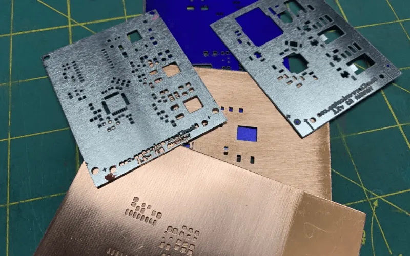
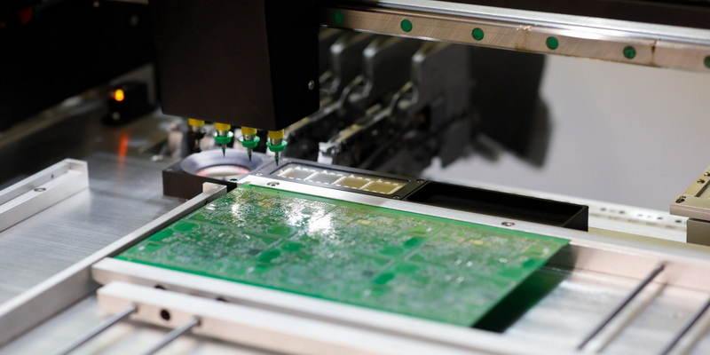
SMT stencils are thin, flat sheets of metal or other materials with precise openings that correspond to the pads on a PCB. They are used in the solder paste printing process to apply solder paste onto PCBs before component placement. The quality of the solder paste printing directly influences the rate of soldering defects, with up to 70% of defects attributed to printing quality issues. Therefore, selecting the right material for the stencil is crucial to ensure optimal print performance and minimize defects.
Common Materials Used for SMT Stencils
Stainless Steel
Stainless steel is the most widely used material for SMT stencils due to its durability, resistance to corrosion, and excellent print quality. It offers several advantages:
- Durability and Long Lifespan: Stainless steel stencils can withstand numerous print cycles without significant degradation.
- Compatibility: They are compatible with most solder pastes and cleaning agents, making them versatile for various applications.
- Dimensional Stability: Stainless steel maintains its shape well, ensuring consistent solder paste deposition.
- Cost-Effectiveness: Compared to other materials, stainless steel is generally more affordable.
However, standard stainless steel may be prone to thickness variations and warping due to heat from laser cutting. Premium and fine-grain stainless steel options are available to mitigate these issues by maintaining tight thickness tolerances and reducing grain size for smoother stencil walls.
Nickel
Nickel stencils, particularly electroformed nickel, are gaining popularity for their unique properties:
- Smooth Aperture Walls: Nickel provides improved paste release due to its smooth aperture walls.
- High Durability: Nickel stencils are more durable and resistant to wear compared to stainless steel.
- Ultra-Fine Pitch Applications: They are suitable for components with very small pitches.
- Longer Lifespan: Nickel stencils generally outlast stainless steel ones.
Despite these advantages, nickel stencils are more expensive than stainless steel and may require specialized handling and storage.
Polyimide (Kapton)
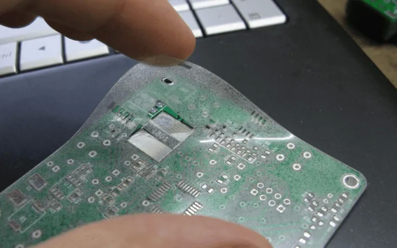
Polyimide, such as Kapton, is another material used for SMT stencils, especially in prototyping or low-volume production. It offers excellent heat resistance and dimensional stability, making it ideal for applications where thermal stability is crucial. However, polyimide stencils are less durable than metal stencils and may not be suitable for high-volume production.
Design Considerations for SMT Stencils
Effective stencil design is crucial for achieving high-quality solder paste prints and minimizing defects. Key considerations include:
Aperture Size and Shape
The size and shape of stencil apertures should match the PCB pads while accounting for the solder paste's properties and desired solder joint profile. Common aperture shapes include rectangles, circles, and home plates. Designers must adhere to minimum aperture width and pitch guidelines to ensure proper paste release and prevent bridging.
Aspect Ratio and Area Ratio
According to the IPC-7525 standard, two critical parameters for determining stencil print performance are the aspect ratio (aperture width / stencil thickness) and area ratio (surface area of the aperture / surface area of the aperture walls). The lowest acceptable aspect ratio is typically 1.5, and the area ratio should be at least 0.66. A higher area ratio generally results in better paste release.
Stencil Thickness
Selecting the appropriate stencil thickness is critical for achieving optimal solder paste volume and print quality. Thinner stencils are ideal for fine-pitch components but may struggle with sufficient paste volume, while thicker stencils can provide robust deposits but may hinder paste release. Manufacturers must balance thickness based on PCB design, component specifications, and solder paste characteristics.

Role of an SMT Process Engineer in Stencil Design
An SMT process engineer plays a vital role in ensuring that stencils are designed and manufactured to meet specific assembly requirements. Their responsibilities include:
- Material Selection: Choosing the appropriate material based on the PCB layout, component specifications, and solder paste characteristics.
- Design Optimization: Ensuring that stencil apertures are correctly sized and shaped to match component pads and accommodate paste shrinkage.
- Process Optimization: Implementing techniques like nano-coating or electropolishing to enhance paste release and print quality.
- Quality Control: Conducting regular inspections to verify stencil quality and performance.
Industry Standards and Best Practices
Industry standards such as IPC-7525B provide guidelines for stencil design, though these are often interpreted differently by manufacturers. It is essential to work closely with stencil suppliers to ensure designs meet specific application needs, especially for complex components like BGAs (Ball Grid Arrays) and fine-pitch devices.
Stencil Manufacturing Techniques
Laser Cutting
Laser cutting is the most common and precise method for creating stencil apertures. High-powered lasers are used to cut the desired aperture shapes and sizes into the stencil material, offering excellent accuracy and repeatability. This method is ideal for creating fine-pitch apertures and complex designs.
Chemical Etching
Chemical etching is an alternative process that involves using a photoresist mask and chemical solution to create apertures. While less precise than laser cutting, it can be cost-effective for larger apertures or thicker stencils.
Stencil Maintenance and Cleaning
Proper maintenance and cleaning of SMT stencils are essential for ensuring consistent print quality and extending the stencil's lifespan. Best practices include:
- Regular Cleaning: Implement a regular cleaning schedule to remove solder paste residue and prevent aperture clogging. Cleaning methods may include manual wiping with solvents, ultrasonic cleaning, or automated stencil cleaning systems.
- Inspection: Regularly inspect stencils for damage, wear, or aperture clogging to maintain print quality. Use magnification tools to examine apertures for any signs of deformation or blockage.
- Proper Storage: Store stencils in a clean, dry environment and use protective covers to prevent damage during handling and transportation. Proper storage helps maintain the stencil's integrity and prolongs its useful life.
Optimizing Stencil Performance
To achieve the best results with SMT stencils, consider the following optimization techniques:
- Nano-coating: Applying a nano-coating to the stencil surface can improve paste release and reduce the need for frequent cleaning. This treatment enhances the stencil's hydrophobic properties, making it easier for solder paste to separate from the aperture walls.
- Electropolishing: Electropolishing the stencil surface can smooth out microscopic imperfections, improving paste release and print quality. This process can be particularly beneficial for fine-pitch applications where consistent paste deposition is critical.
- Custom Aperture Designs: For challenging components or unique PCB layouts, custom aperture designs can be implemented to optimize paste deposition. This may include modified shapes, stepped apertures, or specialized patterns to address specific printing requirements.
Future Trends in SMT Stencil Technology
As electronics continue to evolve, SMT stencil technology is advancing to meet new challenges:
- D-Printed Stencils: Additive manufacturing techniques are being explored for creating complex, multi-level stencils that can accommodate a wide range of component types and sizes on a single PCB.
- Smart Stencils: Integration of sensors and data collection capabilities into stencils could provide real-time feedback on print quality and stencil performance, enabling proactive maintenance and process optimization.
Conclusion
Material selection is a pivotal factor in the effectiveness of SMT stencils, impacting print quality, durability, and compatibility. Stainless steel and nickel are the primary materials used, each with its advantages and applications. An SMT process engineer's expertise is crucial in optimizing stencil design and ensuring that the chosen material aligns with the specific requirements of the PCB assembly process.

FAQ
1. What are the most common materials used for SMT stencils?
The most common materials used for SMT stencils are stainless steel and nickel. Stainless steel is preferred for its durability and cost-effectiveness, while nickel is chosen for its smooth aperture walls and high durability.
2. How does the aspect ratio affect stencil performance?
The aspect ratio (aperture width / stencil thickness) affects stencil performance by determining the ease of solder paste release. A higher aspect ratio can improve paste release but may compromise paste volume.
3. What role does an SMT process engineer play in stencil design?
An SMT process engineer is responsible for selecting the appropriate material, optimizing stencil design, implementing process enhancements, and ensuring quality control to meet specific assembly requirements.
4. What are some future trends in SMT stencil technology?
Future trends include the use of additive manufacturing for complex stencils and the integration of sensors to create smart stencils that provide real-time feedback on print quality.
5. How does stencil thickness impact print quality?
Stencil thickness impacts print quality by influencing the volume of solder paste deposited. Thicker stencils provide more robust deposits but may hinder paste release, while thinner stencils are ideal for fine-pitch components but may struggle with sufficient paste volume.
Citations:
[1] https://rigidflexpcb.org/comprehensive-guide-to-smt-stencils/
[2] https://pcbpit.com/smt-stencil-a-comprehensive-guide/
[3] https://dinamike-solution.com/2024/10/14/guide-to-smt-stencil-types-benefits-and-applications/
[4] https://www.ipc.org/system/files/technical_resource/E38&S12-02%20-%20Chrys%20Shea.pdf
[5] https://www.circuitinsight.com/pdf/selecting_stencil_technologies_optimize_print_performance_ipc.pdf
[6] https://iconnect007.com/article/118546/smt-stencils-101-what-are-industrystandard-stencil-designs/118549/smt
[7] https://smtnet.com/library/files/upload/plastic-vs-metal-stencils.pdf
[8] https://www.reddit.com/r/AskElectronics/comments/pk71xl/how_to_design_pcb_stencil_to_optimize_solder/
[9] https://www.raypcb.com/laser-cut-stencils-and-chemical-etching-stencils/


