Content Menu
● The Fundamentals of SMT PCB AOI
>> Key Features of SMT PCB AOI Systems
● The Critical Role of AOI in SMT Assembly
>> Pre-reflow Inspection
>> Post-reflow Inspection
>> Final Quality Assurance
● The Impact of AOI on Manufacturing Efficiency
>> Increased Throughput
>> Early Defect Detection
>> Reduced Labor Costs
>> Improved Consistency
● China's SMT PCB AOI Industry: A Global Powerhouse
>> Market Size and Growth
>> Domestic Innovation and Competition
>> Challenges and Opportunities
● Advanced Features of Modern SMT PCB AOI Systems
>> Artificial Intelligence and Machine Learning
>> 3D Inspection Capabilities
>> Multi-angle Inspection
>> Integration with Industry 4.0
● Best Practices for Implementing SMT PCB AOI
● Future Trends in SMT PCB AOI Technology
● Conclusion
● FAQ
>> 1. What are the main advantages of using SMT PCB AOI in electronics manufacturing?
>> 2. How does China's SMT PCB AOI market compare to the global market?
>> 3. What are some common defects that SMT PCB AOI can detect?
>> 4. How is AI being integrated into SMT PCB AOI systems?
>> 5. What future developments can we expect in SMT PCB AOI technology?
● Citations:
In the rapidly evolving landscape of modern electronics manufacturing, quality control and efficiency are paramount. As devices become smaller, more complex, and increasingly integrated into our daily lives, the need for precise and reliable manufacturing processes has never been greater. One technology that has emerged as a crucial component in ensuring the quality and reliability of electronic products is the Automated Optical Inspection (AOI) system, specifically designed for Surface Mount Technology (SMT) Printed Circuit Board (PCB) production. This article will explore the significant role that SMT PCB AOI plays in contemporary electronics manufacturing, with a particular focus on its implementation and impact in China, a global leader in electronics production.

The Fundamentals of SMT PCB AOI
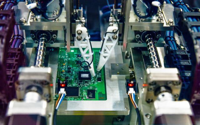
SMT PCB AOI is an advanced inspection technology that uses high-resolution cameras and sophisticated image processing algorithms to detect defects and ensure quality in PCB assembly[1]. This automated system is designed to identify a wide range of issues, from component placement errors to solder joint defects, with a level of precision and speed that far surpasses manual inspection methods.
Key Features of SMT PCB AOI Systems
1. High-resolution imaging: AOI machines utilize state-of-the-art cameras to capture detailed images of PCBs.
2. Advanced algorithms: Sophisticated software analyzes the captured images to detect anomalies and defects.
3. Real-time inspection: AOI systems can perform inspections in-line with the production process, allowing for immediate detection of issues.
4. Customizable parameters: Manufacturers can set specific criteria for inspection based on their unique requirements.
The Critical Role of AOI in SMT Assembly
In the context of SMT assembly, AOI plays a multifaceted and indispensable role. Its implementation at various stages of the production process ensures comprehensive quality control and contributes significantly to the overall efficiency of manufacturing operations[4].
Pre-reflow Inspection
Before the reflow soldering process, AOI systems can inspect:
- Component placement accuracy
- Orientation of components
- Presence of all required components
- Solder paste deposition quality
Post-reflow Inspection
After reflow soldering, AOI is crucial for checking:
- Solder joint quality
- Component shifts during reflow
- Bridging or shorts between solder joints
- Missing or misaligned components
Final Quality Assurance
As a final step, AOI can perform a comprehensive inspection of the entire PCB assembly, ensuring that all aspects meet the required specifications before the product moves to the next stage of production or packaging.
The Impact of AOI on Manufacturing Efficiency
The integration of AOI systems into SMT PCB production lines has revolutionized the manufacturing process, offering numerous benefits that contribute to increased efficiency and reduced costs[1][4].
Increased Throughput
AOI systems can inspect PCBs at a much faster rate than manual inspection methods, allowing for higher production volumes without compromising on quality.
Early Defect Detection
By identifying issues early in the production process, AOI helps prevent defective components from progressing through subsequent manufacturing stages, saving time and resources.
Reduced Labor Costs
Automation of the inspection process reduces the need for manual labor, allowing skilled workers to focus on more complex tasks and problem-solving.
Improved Consistency
AOI systems provide consistent and objective inspection results, eliminating the variability associated with human inspectors and ensuring uniform quality standards across production runs.
China's SMT PCB AOI Industry: A Global Powerhouse
China has emerged as a dominant force in the global electronics manufacturing industry, and its adoption of advanced technologies like SMT PCB AOI has played a significant role in maintaining this position[2].
Market Size and Growth
In 2017, the Chinese AOI market was valued at RMB9.52 billion, representing a substantial 21.7% of the global AOI market size[2]. This impressive market share underscores China's commitment to implementing cutting-edge inspection technologies in its manufacturing processes.
Domestic Innovation and Competition
While foreign companies initially dominated the Chinese AOI equipment market, domestic players have made significant strides in recent years[2]. Companies like Aleader, Jutze Intelligence, and Ekt-Tech have emerged as competitive forces, focusing on downstream processes such as PCB inspection.
Challenges and Opportunities
Despite the growth of domestic AOI manufacturers, Chinese firms still face challenges in terms of R&D capabilities and technological innovation[2]. This presents both a challenge and an opportunity for the Chinese SMT PCB AOI industry to invest in research and development to close the gap with international competitors.

Advanced Features of Modern SMT PCB AOI Systems
As technology continues to advance, SMT PCB AOI systems are becoming increasingly sophisticated, offering new features that enhance their capabilities and effectiveness in modern electronics manufacturing[1][4].
Artificial Intelligence and Machine Learning
Many modern AOI systems incorporate AI and machine learning algorithms to improve defect detection accuracy and reduce false positives. These systems can learn from historical data and adapt to new types of defects over time.
3D Inspection Capabilities
Advanced AOI machines now offer 3D inspection capabilities, allowing for more accurate assessment of component heights, solder joint quality, and overall board planarity.
Multi-angle Inspection
Some AOI systems use multiple cameras or adjustable angles to inspect components and solder joints from various perspectives, providing a more comprehensive evaluation of PCB quality.
Integration with Industry 4.0
AOI systems are increasingly being integrated into broader Industry 4.0 initiatives, allowing for real-time data sharing, predictive maintenance, and enhanced process control across the entire manufacturing line.
Best Practices for Implementing SMT PCB AOI
To maximize the benefits of SMT PCB AOI in electronics manufacturing, companies should consider the following best practices:
1. Proper training: Ensure that operators and technicians are well-trained in using and maintaining AOI equipment.
2. Regular calibration: Maintain the accuracy of AOI systems through regular calibration and maintenance.
3. Continuous improvement: Use data gathered from AOI systems to drive continuous improvement in manufacturing processes.
4. Integration with other systems: Integrate AOI data with other quality control and manufacturing execution systems for a holistic approach to quality management.
5. Customization: Tailor AOI parameters and algorithms to specific product requirements and manufacturing processes.
Future Trends in SMT PCB AOI Technology
As the electronics manufacturing industry continues to evolve, so too will SMT PCB AOI technology. Some emerging trends to watch include:
1. Enhanced AI capabilities for more accurate defect classification and reduced false positives.
2. Integration of augmented reality (AR) for improved operator interaction and defect visualization.
3. Development of more compact and flexible AOI systems to accommodate diverse production environments.
4. Increased use of big data analytics to derive deeper insights from AOI inspection results.
5. Further integration with other inspection technologies, such as X-ray and thermal imaging, for more comprehensive quality control.
Conclusion
SMT PCB AOI has become an indispensable tool in modern electronics manufacturing, playing a crucial role in ensuring product quality, improving efficiency, and reducing costs. As the industry continues to push the boundaries of miniaturization and complexity, the importance of advanced inspection technologies like AOI will only grow. China's significant market share and ongoing investment in this technology underscore its critical role in maintaining the country's position as a global leader in electronics manufacturing.
The future of SMT PCB AOI looks promising, with ongoing advancements in AI, machine learning, and 3D inspection capabilities set to further enhance its effectiveness. As manufacturers continue to adopt and refine these technologies, we can expect to see even higher levels of quality and efficiency in electronics production, ultimately benefiting consumers with more reliable and innovative electronic devices.

FAQ
1. What are the main advantages of using SMT PCB AOI in electronics manufacturing?
SMT PCB AOI offers several key advantages in electronics manufacturing:
- Increased inspection speed and accuracy compared to manual methods
- Early detection of defects, reducing waste and rework costs
- Consistent and objective inspection results
- Ability to handle high-volume production with maintained quality
- Real-time feedback for process improvement
2. How does China's SMT PCB AOI market compare to the global market?
China's SMT PCB AOI market is a significant player on the global stage:
- In 2017, China's AOI market was worth RMB9.52 billion
- This represented 21.7% of the global AOI market size
- The market has seen rapid growth, with a 10.3% increase from the previous year
- Chinese domestic manufacturers are increasingly competing with international firms
3. What are some common defects that SMT PCB AOI can detect?
SMT PCB AOI systems are designed to detect a wide range of defects, including:
- Component misalignment or absence
- Solder bridging or insufficient solder
- Polarity issues with components
- Lifted leads or components
- Foreign object debris (FOD) on the PCB
- Solder paste volume and position errors
4. How is AI being integrated into SMT PCB AOI systems?
AI is enhancing SMT PCB AOI systems in several ways:
- Improved defect detection accuracy through machine learning algorithms
- Adaptive inspection parameters based on historical data
- Reduction of false positives and negatives
- Enhanced pattern recognition for new defect types
- Predictive maintenance of AOI equipment
5. What future developments can we expect in SMT PCB AOI technology?
The future of SMT PCB AOI technology is likely to include:
- More advanced 3D inspection capabilities
- Integration with augmented reality for improved operator interaction
- Enhanced AI and machine learning for more accurate defect classification
- Greater integration with other inspection technologies (e.g., X-ray, thermal imaging)
- Increased use of big data analytics for process optimization
Citations:
[1] https://www.neodensmt.com/news/how-does-smt-aoi-machine-work-74092002.html
[2] http://www.researchinchina.com/Htmls/Report/2018/10468.html
[3] https://smtnet.com/library/index.cfm?fuseaction=browse_articles&cat=all&start_at=281&maxrows=10
[4] https://www.zjyingxing.com/info/what-is-the-role-of-aoi-machines-in-the-smt-in-91506284.html
[5] https://etasmt.en.made-in-china.com/product/uQspdoUxagVL/China-SMT-PCB-Aoi-Optical-Inspection-Equipment-Component-Inspector-Machine.html
[6] https://www.electronicsforu.com/market-verticals/industrial/automated-optical-inspection-smt-environment
[7] https://www.grande-pcba.com/the-role-of-aoi-in-smt-assembly/
[8] https://gdxinling.en.made-in-china.com/product-group/ieufZMNbrzWP/SMT-AOI-catalog-1.html
[9] https://www.7pcb.com/blog/differences-between-aoi-and-spi-in-smt-assembly


