Content Menu
● Introduction
● The Stages of SMT Manufacturing
>> Design and Preparation
>> Solder Paste Printing
>> Component Placement
>> Reflow Soldering
>> Inspection and Testing
>> Rework and Repair
>> Final Assembly and Packaging
● Benefits of SMT Manufacturing
● Challenges in SMT Manufacturing
● Conclusion
● Related Questions
>> 1. What types of components are used in SMT?
>> 2. How does reflow soldering work?
>> 3. What are common defects in SMT manufacturing?
>> 4. Why is automated optical inspection important?
>> 5. What industries commonly use SMT?
Introduction
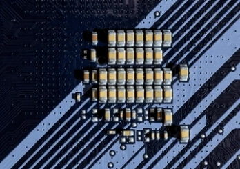
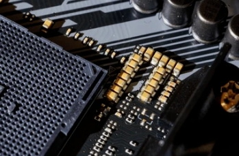
Surface Mount Technology (SMT) is a modern method for assembling electronic components onto printed circuit boards (PCBs). Unlike traditional through-hole technology, where components are inserted into holes on the PCB, SMT allows components to be mounted directly onto the surface of the board. This innovative approach has revolutionized the electronics manufacturing industry, enabling faster production times, reduced costs, and improved performance of electronic devices. In this article, we will explore the SMT manufacturing process in detail, discussing its various stages, benefits, and challenges.

The Stages of SMT Manufacturing
The SMT manufacturing process consists of several key stages, each critical to ensuring the quality and reliability of the final product. These stages include:
Design and Preparation
Before any manufacturing can take place, the design of the PCB must be completed. This involves creating a schematic diagram that outlines how the electronic components will be arranged on the board. Once the design is finalized, a bill of materials (BOM) is created to list all components needed for production.
Afterward, the PCB layout is designed using specialized software. This layout determines where each component will be placed on the board and ensures that there is enough space for soldering and other processes. The design must also consider factors such as signal integrity and thermal management.
Solder Paste Printing
The first physical step in the SMT process is solder paste printing. Solder paste is a mixture of tiny solder balls and flux that is used to attach components to the PCB. A stencil is created based on the PCB layout, which allows solder paste to be applied only to specific areas where components will be placed.
The stencil is aligned with the PCB, and solder paste is spread across it using a squeegee. This process ensures that an appropriate amount of solder paste is deposited onto each pad on the PCB. Proper application of solder paste is crucial, as insufficient or excessive paste can lead to defects in solder joints.
Component Placement
Once solder paste has been applied, the next step is component placement. Automated machines known as pick-and-place machines are used for this purpose. These machines are equipped with robotic arms that pick up surface mount devices (SMDs) from their reels or trays and place them precisely onto the solder paste-covered pads on the PCB.
The accuracy of component placement is vital for ensuring proper electrical connections and minimizing defects during soldering. Advanced pick-and-place machines use vision systems to inspect each component's position before final placement, allowing for adjustments if necessary.
Reflow Soldering
After all components have been placed on the PCB, it undergoes reflow soldering. This process involves heating the entire assembly to melt the solder paste, which then solidifies to form strong electrical connections between the components and the PCB.
Reflow ovens are typically used for this purpose. The PCBs pass through different temperature zones within the oven: preheating, soaking, reflowing, and cooling. Each zone serves a specific purpose in ensuring that the solder melts evenly and adheres properly to both the components and the board.
Inspection and Testing
Once reflow soldering is complete, it is essential to inspect and test the assembled PCBs for defects. Various inspection methods can be employed:
- Visual Inspection: Operators visually check each board for obvious defects such as misplaced components or insufficient solder.
- Automated Optical Inspection (AOI): Machines equipped with cameras scan each PCB to identify defects based on predefined criteria.
- X-ray Inspection: For complex assemblies with hidden solder joints, X-ray inspection may be used to ensure proper connections beneath components.
After inspection, functional testing is performed to verify that each assembled PCB operates correctly according to its specifications.

Rework and Repair
Despite rigorous inspection processes, some defects may still occur during SMT manufacturing. Rework stations are set up to address these issues by allowing operators to remove faulty components and replace them with new ones. This process requires specialized tools such as hot air rework stations or laser removal systems.
Rework is essential for maintaining high-quality standards in electronics manufacturing but can add time and cost to production if not managed properly.
Final Assembly and Packaging
Once all PCBs have passed inspection and any necessary rework has been completed, they undergo final assembly processes such as adding connectors or other mechanical elements required for functionality. After assembly, PCBs are packaged carefully to prevent damage during shipping.
Benefits of SMT Manufacturing
The SMT manufacturing process offers numerous advantages over traditional methods:
- Higher Component Density: SMT allows for smaller components to be used and placed closer together on a PCB, enabling more compact designs.
- Improved Performance: The shorter electrical paths associated with surface-mounted components can lead to better performance in terms of speed and signal integrity.
- Cost Efficiency: The automated nature of SMT reduces labor costs and increases production speed, making it more cost-effective than manual assembly methods.
- Flexibility: SMT can accommodate a wide variety of component types and sizes, making it suitable for diverse applications across industries.
Challenges in SMT Manufacturing
While SMT offers many benefits, it also presents challenges that manufacturers must navigate:
- Component Handling: SMDs are often smaller and more fragile than through-hole components, requiring careful handling during placement and assembly.
- Thermal Management: The compact nature of SMT designs can lead to heat dissipation issues; effective thermal management solutions must be implemented.
- Defect Rates: Despite advanced inspection techniques, defect rates can still pose challenges; continuous improvement processes are necessary to minimize these issues.
Conclusion
In summary, Surface Mount Technology has transformed electronics manufacturing by enabling faster production times and higher component densities while reducing costs. Understanding each stage of the SMT manufacturing process—from design through final assembly—is crucial for manufacturers aiming to produce high-quality electronic devices efficiently. As technology continues to evolve, SMT will likely play an even more significant role in shaping the future of electronics production.

Related Questions
1. What types of components are used in SMT?
SMT utilizes various types of components known as surface mount devices (SMDs), including resistors, capacitors, integrated circuits (ICs), diodes, and connectors.
2. How does reflow soldering work?
Reflow soldering involves heating an assembled PCB in a controlled manner within a reflow oven so that solder paste melts and forms solid connections between components and pads when cooled.
3. What are common defects in SMT manufacturing?
Common defects include insufficient solder joints, misaligned components, tombstoning (where one end of a component lifts off), and bridging (unintended connections between pads).
4. Why is automated optical inspection important?
Automated optical inspection (AOI) helps detect defects early in the manufacturing process by comparing images of assembled boards against predefined standards before they proceed further down the line.
5. What industries commonly use SMT?
SMT is widely used across various industries including consumer electronics, automotive electronics, telecommunications equipment, medical devices, and industrial automation systems.


