Content Menu
● Understanding SMT and Its Importance
● What is Automated Optical Inspection (AOI)?
● How Does AOI Work?
● Benefits of Implementing AOI in PCB Manufacturing
>> 1. Early Detection of Defects
>> 2. Increased Throughput
>> 3. Consistency and Repeatability
>> 4. Data Collection and Analysis
>> 5. Cost Efficiency
● Challenges in Implementing AOI
>> 1. High Initial Investment
>> 2. Complexity of Set-Up
>> 3. Limitations in Detecting Certain Defects
● Future Trends in AOI Technology
>> 1. Integration with Artificial Intelligence (AI)
>> 2. 3D Inspection Technology
>> 3. IoT Connectivity
● Conclusion
● FAQ
>> 1. What types of defects can AOI detect?
>> 2. How does AOI improve production efficiency?
>> 3. Is there a significant cost associated with implementing AOI?
>> 4. Can AI enhance the capabilities of AOI systems?
>> 5. What future trends should we expect in AOI technology?
Surface Mount Technology (SMT) has revolutionized the electronics manufacturing industry, allowing for the production of smaller, more efficient printed circuit boards (PCBs). As the complexity of PCBs increases, so does the need for effective quality control measures. One of the most significant advancements in this area is Automated Optical Inspection (AOI). This article will explore what SMT Automated Optical Inspection is, how it works, and its impact on improving PCB quality.

Understanding SMT and Its Importance
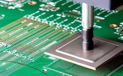
Surface Mount Technology refers to a method of mounting electronic components directly onto the surface of a PCB. Unlike traditional through-hole technology, where components are inserted into holes and soldered from the opposite side, SMT allows for a more compact design. This method has several advantages:
- Space Efficiency: SMT components are generally smaller and can be placed closer together on a PCB.
- Increased Reliability: With fewer mechanical connections, SMT reduces the likelihood of failure due to vibration or thermal cycling.
- Higher Production Speed: SMT allows for faster assembly processes, which is crucial for meeting market demands.
Given these advantages, it is essential to ensure that SMT processes maintain high-quality standards.
What is Automated Optical Inspection (AOI)?
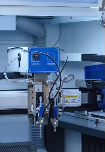
Automated Optical Inspection is a non-contact inspection method that uses cameras and sophisticated software to analyze PCBs during various stages of production. AOI systems can detect defects such as:
- Missing components
- Misaligned components
- Solder joint issues
- Component orientation errors
By identifying these defects early in the manufacturing process, AOI helps prevent costly rework and ensures that only high-quality products reach consumers.
How Does AOI Work?
The AOI process involves several key steps:
1. Image Acquisition: High-resolution cameras capture images of the PCB at various angles. Some systems utilize multiple cameras to create a comprehensive view.
2. Image Processing: The captured images are processed using advanced algorithms that compare them against predefined standards or templates. This step involves:
- Edge detection to identify component outlines
- Pattern recognition to verify component types and placements
3. Defect Detection: The system identifies discrepancies between the captured images and the expected results. This includes checking for:
- Missing or misplaced components
- Incorrect soldering
4. Reporting: Any detected defects are logged, and operators receive alerts to address issues immediately.
Benefits of Implementing AOI in PCB Manufacturing
Implementing AOI systems in PCB manufacturing offers numerous benefits that contribute to improved quality:
1. Early Detection of Defects
One of the most significant advantages of AOI is its ability to identify defects early in the manufacturing process. Early detection minimizes the risk of defective products reaching customers and reduces overall production costs.
2. Increased Throughput
AOI systems operate at high speeds and can inspect multiple boards simultaneously. This capability increases throughput without sacrificing quality, allowing manufacturers to meet tight deadlines.

3. Consistency and Repeatability
Unlike manual inspection methods, which can be prone to human error, AOI provides consistent and repeatable results. This reliability enhances overall quality assurance processes.
4. Data Collection and Analysis
AOI systems generate valuable data that can be used for continuous improvement initiatives. Manufacturers can analyze defect trends over time to identify root causes and implement corrective actions.
5. Cost Efficiency
By reducing rework rates and improving yield, AOI contributes to significant cost savings in PCB manufacturing. The initial investment in AOI technology often pays off quickly through increased efficiency and reduced waste.
Challenges in Implementing AOI
While AOI offers many benefits, there are also challenges associated with its implementation:
1. High Initial Investment
The cost of purchasing and integrating AOI systems can be substantial, particularly for small manufacturers. However, this investment is often justified by long-term savings.
2. Complexity of Set-Up
Setting up an AOI system requires careful calibration and programming to ensure accurate inspections. Manufacturers must invest time and resources into training personnel.
3. Limitations in Detecting Certain Defects
While AOI is effective at identifying many types of defects, it may not detect all issues, such as certain types of internal solder joint problems or hidden defects under components.
Future Trends in AOI Technology
The field of Automated Optical Inspection continues to evolve with advancements in technology:
1. Integration with Artificial Intelligence (AI)
AI algorithms are being integrated into AOI systems to enhance defect detection capabilities further. Machine learning can improve pattern recognition over time, making inspections more accurate.
2. 3D Inspection Technology
Emerging 3D inspection technologies allow for better analysis of complex PCBs by providing depth perception alongside traditional 2D imaging.
3. IoT Connectivity
As manufacturers adopt Industry 4.0 practices, integrating AOI systems with IoT platforms will enable real-time monitoring and data sharing across production lines.
Conclusion
In conclusion, SMT Automated Optical Inspection plays a critical role in enhancing PCB quality by providing early defect detection, increasing throughput, ensuring consistency, collecting valuable data, and contributing to cost efficiency. Despite some challenges associated with implementation, the benefits far outweigh the drawbacks for most manufacturers. As technology continues to advance, we can expect even greater improvements in inspection capabilities that will further elevate industry standards.

FAQ
1. What types of defects can AOI detect?
AOI can detect various defects including missing components, misalignment issues, solder joint problems, and incorrect component orientations.
2. How does AOI improve production efficiency?
By identifying defects early in the manufacturing process, AOI reduces rework rates and allows for faster production speeds without compromising quality.
3. Is there a significant cost associated with implementing AOI?
Yes, while there is an initial investment required for purchasing and setting up AOI systems, the long-term savings from increased efficiency often justify this cost.
4. Can AI enhance the capabilities of AOI systems?
Absolutely! Integrating AI into AOI systems improves defect detection accuracy through advanced pattern recognition and machine learning techniques.
5. What future trends should we expect in AOI technology?
Future trends include greater integration with AI technologies, advancements in 3D inspection capabilities, and enhanced connectivity through IoT platforms for real-time monitoring.


