Content Menu
● What is SMT?
>> Key Features of SMT
● What is an SMT Stencil?
>> Types of SMT Stencils
>> Manufacturing Processes
>>> Precision Techniques
● Applications of SMT Stencils
● Advantages of Using SMT Stencils
>> Enhanced Efficiency
>> Flexibility and Adaptability
● Challenges Associated with SMT Stencils
● Future Trends in SMT Stencil Technology
>> Nano-coatings and Surface Treatments
>> Additive Manufacturing and Customization
>> Environmental Considerations
● Conclusion
● FAQ
>> 1. What materials are used to make SMT stencils?
>> 2. How do I clean an SMT stencil?
>> 3. Can I use an SMT stencil for different PCB designs?
>> 4. What is the difference between laser-cut and electroformed stencils?
>> 5. How does using an SMT stencil improve production efficiency?
● Citations:
Surface Mount Technology (SMT) stencils are essential tools in the electronics manufacturing process, specifically for the assembly of printed circuit boards (PCBs). These stencils play a critical role in applying solder paste to the pads of a PCB, ensuring that components can be accurately and securely attached during the soldering process. This article delves into the definition, types, manufacturing processes, applications, advantages, challenges, and future trends associated with SMT stencils.

What is SMT?
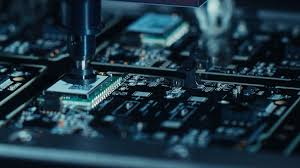
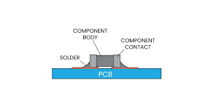
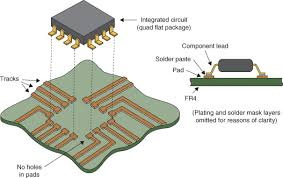
Before discussing SMT stencils, it is important to understand what Surface Mount Technology (SMT) entails. SMT is a method used to mount electronic components directly onto the surface of PCBs. Unlike traditional through-hole technology, where components are inserted into holes drilled in the PCB, SMT allows for a more compact design and higher component density.
Key Features of SMT
- Compact Design: SMT enables smaller and lighter circuit boards.
- Higher Component Density: More components can be placed on a single board.
- Automated Assembly: SMT processes are highly automated, increasing efficiency and reducing labor costs.
What is an SMT Stencil?
An SMT stencil is a thin sheet made from materials such as stainless steel or polymer, with openings cut out in specific patterns that correspond to the pads on a PCB. The stencil is used to apply solder paste to these pads before the components are placed on the board.
Types of SMT Stencils
SMT stencils can be categorized based on various factors:
- Laser-Cut Stencils: Made using laser technology for high precision and intricate designs.
- Electroformed Stencils: Created through an electroforming process that allows for very fine apertures and high durability.
- Metal Stencils: Typically made from stainless steel, offering strength and longevity.
- Plastic Stencils: Made from flexible materials suitable for low-volume production or prototyping.
- Framed and Frameless Stencils: Framed stencils are fixed in a frame for stability during high-volume printing, while frameless stencils are more portable and cost-effective for smaller runs.
Manufacturing Processes
The manufacturing of SMT stencils involves several steps:
1. Design Creation: Using CAD software to create a design that matches the PCB layout.
2. Aperture Cutting: The stencil material is cut using laser or chemical etching techniques to create openings that match the pad sizes on the PCB.
3. Finishing Touches: Edges are smoothed out, and any additional features like alignment holes are added.
4. Quality Control: The stencil undergoes rigorous testing to ensure accuracy and quality before being sent for use in production.
Precision Techniques
- Laser Cutting: High-energy laser beams create precise aperture walls, ensuring sharp edges. This method is known for its accuracy in defining solder paste deposition areas, vital for reliable electrical connections.
- Chemical Etching: This involves selectively removing material using chemical solutions. It allows for intricate aperture designs with precise tolerances, accommodating complex PCB layouts and fine-pitch components.
Applications of SMT Stencils
SMT stencils are primarily used in PCB assembly processes. Their applications include:
- Solder Paste Application: The primary use of SMT stencils is to apply solder paste accurately onto PCB pads.
- Component Placement: After applying solder paste, components are placed onto the board before being soldered.
- Rework Processes: Stencils can also be used in rework processes where components need to be replaced or repaired.
Advantages of Using SMT Stencils
Using SMT stencils offers several benefits:
- Precision: Stencils ensure accurate application of solder paste, reducing defects and improving yield rates. This precision is essential for maintaining reliable electrical connections.
- Consistency: Automated stencil printing leads to uniformity across multiple boards, which enhances product quality.
- Efficiency: The use of stencils speeds up the assembly process compared to manual soldering techniques. By enabling simultaneous solder paste application across multiple PCBs, manufacturers can significantly reduce assembly time and meet tight deadlines.

Enhanced Efficiency
Stencils streamline the PCB assembly process by enabling simultaneous solder paste application across multiple PCBs. This reduces assembly time, accelerates production throughput, and helps manufacturers meet tight deadlines and delivery schedules. Enhanced efficiency is crucial for maintaining competitiveness in the fast-paced electronics manufacturing industry, where time-to-market can be a critical factor.
Flexibility and Adaptability
Modern SMT stencil technologies adapt to diverse PCB designs and component configurations. Customizable stencil designs accommodate fine-pitch components, complex layouts, and varying board thicknesses, supporting the integration of new technologies without compromising quality. Flexibility and adaptability are crucial for keeping pace with rapid technological advancements and evolving customer demands.
Challenges Associated with SMT Stencils
While there are many advantages to using SMT stencils, there are also challenges:
- Cost: High-quality stencils can be expensive, particularly for low-volume production runs. However, investing in quality stencils often pays off through improved yield rates and reduced defects.
- Maintenance: Stencils require regular cleaning and maintenance to prevent contamination and ensure longevity. Neglecting this aspect can lead to decreased performance over time.
- Design Limitations: Complex designs may require more intricate stencils, which can complicate manufacturing processes. Additionally, if not properly designed or aligned during application, they may lead to inconsistent results.
Future Trends in SMT Stencil Technology
The evolution of SMT stencil technology continues to drive innovation:
Nano-coatings and Surface Treatments
Advanced nano-coatings improve solder paste release and reduce adhesion, enhancing print quality and fine-pitch component printing. They also require less frequent cleaning, prolonging stencil life. Nano-coatings represent a significant advancement in stencil technology, offering enhanced performance and reduced maintenance requirements.
Additive Manufacturing and Customization
3D printing enables custom-designed SMT stencils with intricate geometries and tailored aperture designs. This flexibility accommodates unique PCB layouts and component configurations. Additive manufacturing allows for the creation of highly specialized stencils that can meet the specific needs of complex and innovative PCB designs.
Environmental Considerations
As sustainability becomes increasingly important in manufacturing processes, SMT stencils contribute by optimizing resource use and reducing material waste. Improved efficiency leads to minimized defects which reduce energy consumption and carbon emissions during production cycles. Companies are now focusing on advanced materials that promote longevity while minimizing environmental impact through eco-friendly practices.
Conclusion
In summary, SMT stencils are crucial tools in modern electronics manufacturing. They facilitate precise application of solder paste, leading to efficient assembly processes and high-quality PCBs. Understanding the types, materials, manufacturing processes, advantages, challenges, and future trends associated with SMT stencils can help manufacturers optimize their production lines and improve overall product quality. As technology advances further into miniaturization and complexity in electronic devices continues to rise, the role of SMT stencils will only become more pivotal in ensuring reliable electronic assemblies that meet consumer demands effectively.

FAQ
1. What materials are used to make SMT stencils?
SMT stencils are typically made from stainless steel or polymer materials. Stainless steel offers durability and precision while polymers may be used for low-volume applications due to their flexibility.
2. How do I clean an SMT stencil?
Cleaning an SMT stencil involves using specialized cleaning solutions designed for removing solder paste residues without damaging the stencil material. Regular cleaning is essential for maintaining stencil performance.
3. Can I use an SMT stencil for different PCB designs?
Yes, but it requires creating a new stencil that matches the specific pad layout of each PCB design. Using an incorrect stencil can lead to poor solder application and assembly defects.
4. What is the difference between laser-cut and electroformed stencils?
Laser-cut stencils are made using laser technology for precise cuts but may have limitations on aperture size; electroformed stencils offer finer apertures with better paste release characteristics but involve a more complex manufacturing process.
5. How does using an SMT stencil improve production efficiency?
Using an SMT stencil automates the solder paste application process which reduces manual labor time while ensuring consistent results across multiple boards; this leads to faster production cycles with lower defect rates.
Citations:
[1] https://jlcpcb.com/blog/guide-to-smt-stencils-in-pcb-assembly
[2] https://rigidflexpcb.org/comprehensive-guide-to-smt-stencils/
[3] https://www.pcbonline.com/blog/guide-to-smt-stencils.html
[4] https://www.epectec.com/smt-stencils/
[5] https://www.twistedtraces.com/blog/understanding-smt-stencils-the-backbone-of-electronics-manufacturing
[6] https://jlcpcb.com/blog/how-to-choose-a-smt-stencil
[7] https://blueringstencils.com/top-5-smt-industry-trends-for-2019/
[8] https://www.pnconline.com/blog/advantages-of-laser-cut-smt-stencils-for-smt-assembly/
[9] https://smartsmttools.com/thicknessofsmtstencils/
[10] https://www.ourpcb.com/smt-stencil.html


