Content Menu
● Understanding SMT Stencil Apertures
>> Key Design Parameters
>> Importance of SMT Stencil Apertures in Electronics Manufacturing
● Innovations in SMT Stencil Aperture Design
>> 1. Advanced Laser Cutting Technologies
>> 2. New Stencil Materials with Fine Grain Structure
>> 3. Optimized Aperture Shapes and Designs
>> 4. Integration of Micro Solder Joint and Aperture Design
>> 5. Ultrasonic and Additive Manufacturing Techniques
● Design Considerations for Future SMT Stencil Apertures
● Future Trends in SMT Stencil Aperture Design
>> Nano-Coatings and Surface Treatments
>> Automated Inspection and Quality Assurance
>> Customization via Additive Manufacturing
>> Environmental and Sustainability Considerations
● Conclusion
● FAQ
>> 1. What are the critical parameters for designing SMT stencil apertures?
>> 2. How does laser technology impact SMT stencil aperture quality?
>> 3. Why are fine grain stencil materials important?
>> 4. What role do aperture shapes play in solder paste printing?
>> 5. How is additive manufacturing influencing SMT stencil aperture design?
Surface Mount Technology (SMT) stencil apertures are critical components in the electronics manufacturing process, directly influencing solder paste deposition quality and, consequently, the reliability of solder joints on printed circuit boards (PCBs). As electronic devices continue to miniaturize and demand higher precision, innovations in SMT stencil aperture design are essential to meet these challenges. This article explores the latest advancements shaping the future of SMT stencil apertures, covering design principles, material innovations, laser cutting technologies, and emerging trends that enhance print quality and assembly efficiency.

Understanding SMT Stencil Apertures
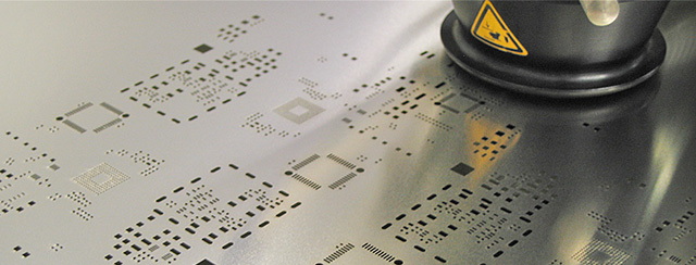
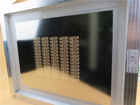
SMT stencil apertures are precisely cut openings in a stencil foil through which solder paste is deposited onto PCB pads. The size, shape, and quality of these apertures determine the volume and distribution of solder paste, which affects the solder joint integrity and overall assembly yield.
Key Design Parameters
Two critical parameters govern stencil aperture design according to IPC standards:
- Aspect Ratio: The ratio of aperture width to stencil thickness, with a minimum acceptable value of 1.5 to ensure proper paste release.
- Area Ratio: The ratio of the aperture surface area to the area of the aperture walls, with a minimum acceptable value of 0.66 to maintain print quality.
As SMT components shrink, maintaining these ratios while ensuring accurate paste deposition becomes increasingly challenging.
Importance of SMT Stencil Apertures in Electronics Manufacturing
The stencil aperture design directly impacts solder paste volume, paste release efficiency, and ultimately the quality of solder joints. Poorly designed apertures can lead to insufficient or excessive solder paste deposits, causing defects such as solder bridging, insufficient solder joints, or tombstoning. Therefore, optimizing SMT stencil apertures is vital for high-yield, high-reliability PCB assembly.
Innovations in SMT Stencil Aperture Design
1. Advanced Laser Cutting Technologies
Recent breakthroughs in laser technology have significantly improved the precision and quality of stencil apertures. The introduction of Single Mode Continuous Wave (CW) Ytterbium Fiber lasers has revolutionized stencil cutting by producing:
- Smaller laser beam diameters (~19 microns)
- Higher energy density (4x increase compared to traditional lasers)
- Programmable pulse/pause ratios for cleaner cuts
These enhancements result in smoother aperture walls, reducing solder paste adhesion to stencil walls and improving paste release during printing. The finer cuts enable the creation of ultra-fine pitch apertures suitable for miniature components like Quad Flat No-lead (QFN) packages and Chip Scale Packages (CSPs).
The precision of these lasers also allows for the cutting of complex aperture shapes that were previously difficult or impossible to achieve with mechanical or older laser cutting methods. This capability supports the trend toward more customized stencil aperture designs tailored to specific component geometries and solder paste behaviors.
2. New Stencil Materials with Fine Grain Structure
Traditional stencil materials like 300 series stainless steel and nickel alloys have limitations in paste release, especially for apertures with low area ratios. Innovations in stencil foil materials now include fine grain stainless steel, which features:
- Smaller grain size and fewer voids
- Reduced solder paste adhesion to aperture walls
- Enhanced paste release and less residue retention
This material advancement allows for printing smaller apertures without compromising stencil thickness or durability, enabling finer pitch printing and higher assembly yields.
Fine grain materials also improve the longevity of stencils by resisting deformation and wear during repeated printing cycles. This durability reduces downtime and maintenance costs in high-volume manufacturing environments.
3. Optimized Aperture Shapes and Designs
Beyond traditional square and round apertures, innovative aperture shapes such as reverse U-shapes, non-convex designs, and trapezoidal apertures are gaining traction. These shapes help control solder paste volume and distribution to prevent common defects like tombstoning (component lifting during reflow) and solder bridging.
For example, reverse U-shape apertures pull solder paste toward the inside of the component pad, increasing paste volume under the part and reducing wetting forces that cause tombstoning. However, designers must carefully consider area ratios when adopting these shapes to maintain print quality.
Other aperture modifications include the use of segmented apertures or "stepped" apertures that vary the aperture opening size within a single pad to optimize paste volume distribution. This approach can improve solder joint reliability without increasing the risk of defects.
4. Integration of Micro Solder Joint and Aperture Design
Emerging patents and research focus on micro solder joint designs where aperture walls do not extend beyond PCB pad edges or component terminals. This precision ensures the formation of non-convex solder joints that improve mechanical strength and electrical connectivity while minimizing solder bridging and defects.
Micro solder joint design involves tailoring the aperture shape and size to the exact geometry of the PCB pad and component terminal, often requiring sub-micron precision in stencil manufacturing. This level of control is critical for next-generation electronics featuring ultra-fine pitch components and high-density interconnects.
5. Ultrasonic and Additive Manufacturing Techniques
The use of ultrasonically activated squeegees during printing has shown to improve paste transfer efficiency, especially for ultra-fine pitch apertures. Ultrasonic vibration reduces the viscosity of solder paste momentarily, allowing it to flow more easily through tiny apertures and improving paste release.
Additionally, additive manufacturing (3D printing) is being explored to create custom stencil apertures with complex geometries tailored to specific PCB layouts, enhancing flexibility and precision in stencil design. 3D printed stencils can incorporate variable thicknesses or embedded features that traditional manufacturing methods cannot achieve, opening new possibilities for solder paste deposition control.

Design Considerations for Future SMT Stencil Apertures
To leverage these innovations, designers must balance multiple factors:
- Aperture Size and Shape: Apertures should be slightly larger than pad dimensions to accommodate solder paste shrinkage and ensure sufficient volume. However, excessive oversizing can cause solder bridging.
- Aperture Wall Smoothness: Smoother walls reduce paste sticking and improve release. Laser cutting advancements and fine grain materials contribute significantly here.
- Material Selection: Fine grain materials enhance paste release and durability, reducing cleaning frequency and extending stencil life.
- Alignment Accuracy: Precise registration between stencil apertures and PCB pads is critical, especially for miniature components with low area ratios. Misalignment can cause insufficient or excessive paste deposits.
- Thermal and Mechanical Stability: Stencil materials and thicknesses must withstand repeated printing cycles without deformation. This stability ensures consistent aperture dimensions and print quality.
- Cleaning and Maintenance: Innovations in stencil coatings and materials reduce solder paste adhesion, decreasing cleaning cycles and extending stencil life.
Future Trends in SMT Stencil Aperture Design
Nano-Coatings and Surface Treatments
Advanced nano-coatings applied to stencil surfaces reduce solder paste adhesion, improving print quality and extending stencil life by reducing cleaning frequency. These coatings create a hydrophobic or non-stick surface that prevents solder paste from sticking to aperture walls, facilitating cleaner paste release.
Such surface treatments also enhance stencil durability by protecting the metal surface from oxidation and wear during cleaning processes.
Automated Inspection and Quality Assurance
Integration of real-time inspection systems into stencil printing processes enables immediate detection of defects such as insufficient paste volume, smearing, or misalignment. Machine vision and AI-powered analytics allow for rapid feedback and corrective actions, ensuring consistent print quality and reducing scrap rates.
Automated inspection can also monitor stencil aperture condition over time, identifying wear or damage before it impacts production quality.
Customization via Additive Manufacturing
3D printing technologies allow for highly customized stencil apertures with intricate shapes and varying thicknesses, supporting complex PCB designs and specialized components. This flexibility enables rapid prototyping and small-batch production of stencils tailored to unique assembly requirements.
Additive manufacturing also opens the door to multi-material stencils that combine metal with polymer or ceramic layers to optimize mechanical and thermal properties.
Environmental and Sustainability Considerations
As electronics manufacturing embraces sustainability, innovations in stencil materials and processes aim to reduce waste and energy consumption. Longer-lasting stencils, reduced cleaning chemicals due to nano-coatings, and additive manufacturing with minimal material waste contribute to greener SMT assembly lines.
Conclusion
Innovations in SMT stencil aperture design are pivotal to meeting the demands of modern electronics manufacturing, where miniaturization and precision are paramount. Advances in laser cutting technology, stencil materials, aperture shapes, and manufacturing methods are collectively enhancing solder paste printing quality, reducing defects, and enabling reliable assembly of ultra-fine pitch components. Emerging technologies such as ultrasonic printing, nano-coatings, and additive manufacturing further expand the capabilities of stencil design, pushing the boundaries of what is possible in SMT assembly.
As these technologies mature, SMT stencil apertures will continue to evolve, driving higher yields, lower costs, and greater flexibility in PCB assembly processes. Manufacturers who adopt these innovations will be better positioned to meet the challenges of next-generation electronics, delivering products with improved reliability and performance.

FAQ
1. What are the critical parameters for designing SMT stencil apertures?
The critical parameters are the aspect ratio (aperture width to stencil thickness, minimum 1.5) and the area ratio (aperture surface area to aperture wall area, minimum 0.66). These ensure proper solder paste release and print quality.
2. How does laser technology impact SMT stencil aperture quality?
Advanced fiber lasers produce smaller beam diameters and higher energy densities, resulting in smoother aperture walls and more precise cuts. This improves solder paste release and enables finer aperture designs for miniature components.
3. Why are fine grain stencil materials important?
Fine grain materials have smaller grains and fewer voids, reducing solder paste adhesion to aperture walls. This facilitates easier paste release, less residue, and allows printing of smaller apertures without reducing stencil thickness.
4. What role do aperture shapes play in solder paste printing?
Aperture shapes like reverse U-shapes control solder paste volume and distribution to prevent defects such as tombstoning by concentrating paste under the component and reducing wetting forces at the edges.
5. How is additive manufacturing influencing SMT stencil aperture design?
3D printing enables the creation of custom stencil apertures with complex geometries tailored to specific PCB layouts, offering greater flexibility and precision in solder paste application.


