Content Menu
● Advancements in Miniaturization and Component Efficiency
>> Smaller Components, Higher Density
>> Adaptive Thermal Management and Hybrid Materials
>> Nanotechnology-Guided Assembly
● Revolutionizing Circuit Boards with Next-Generation SMD Materials
>> Graphene-Infused Composites
>> Ceramic-Polymer Hybrids
>> Flexible Polyimide Substrates
>> Environmental Sustainability in Materials
● Automation and AI in Surface Mount Technology Assembly
>> AI-Powered Optimization
>> Advanced Vision Systems
>> Collaborative Robots (Cobots)
>> Predictive Maintenance and Smart Factories
>> Micron-Level Precision and High-Speed Placement
>> Modular and Flexible Machine Designs
● Emerging Trends and Best Practices for Designers in 2025
>> Adaptive Prototyping and Nano-Precision Design Tools
>> Virtual Collaboration and Cloud-Based Platforms
>> Edge AI Integration in Devices
>> Modular and Scalable Components
>> Eco-Conscious Design
>> Hybrid Manufacturing Techniques
>> Designing for 5G and Beyond
● SIPLACE CA2: A Hybrid Revolution in Placement Machines
>> Integration of Semiconductor and SMT Assembly
>> Benefits for Industry
>> Productivity and Cost Efficiency
● Conclusion
● FAQ
>> 1. What is an automatic SMD pick and place machine?
>> 2. How does AI improve SMD placement machines?
>> 3. What are the challenges faced by modern SMD placement machines?
>> 4. How are new materials impacting SMD placement technology?
>> 5. What future trends will shape SMD placement technology?
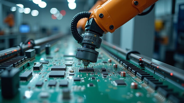
Surface-Mount Device (SMD) placement technology is a cornerstone of modern electronics manufacturing. It enables the precise and efficient assembly of tiny electronic components onto printed circuit boards (PCBs), which are the backbone of virtually all electronic devices today. As consumer demands grow for smaller, faster, and smarter electronics, the technology behind SMD placement machines-especially automatic SMD pick and place systems-has evolved rapidly. In 2025, we are witnessing revolutionary innovations that push the boundaries of speed, precision, flexibility, and sustainability in electronics assembly.

This comprehensive article explores the latest innovations in SMD placement technology, focusing on automatic SMD pick and place machines, the materials used, AI integration, and emerging trends shaping the future of electronics manufacturing.
Advancements in Miniaturization and Component Efficiency
One of the most transformative trends in SMD placement technology is the ongoing miniaturization of components. As electronic devices become more compact and multifunctional, the demand for smaller yet more capable components has skyrocketed. This trend directly influences the design and capabilities of SMD placement machines.
Smaller Components, Higher Density
Modern SMD components are now available in ultra-small packages such as 01005 (0.4mm × 0.2mm) and even smaller. These tiny components allow engineers to design PCBs with much higher component density, enabling more complex circuits in a smaller footprint.
- Challenges for SMD placement machines: Handling and placing these miniature parts requires extreme precision, often down to a few microns. Machines must be equipped with advanced vision systems and ultra-precise robotic arms to avoid misplacement or damage.
- Benefits: Higher density PCBs mean more functionality in smartphones, wearables, IoT devices, and medical implants without increasing size or weight.
Adaptive Thermal Management and Hybrid Materials
As components shrink, managing heat dissipation becomes critical. Innovations in SMD placement technology now include the ability to place components made from hybrid materials that offer better thermal conductivity and mechanical stability.
- Thermally optimized components reduce the risk of overheating.
- Hybrid materials such as metal-ceramic composites improve durability and performance.
Nanotechnology-Guided Assembly
Nanotechnology is increasingly influencing SMD placement machines. By integrating nano-scale sensors and actuators, machines can achieve unprecedented placement accuracy and quality control.
- Nano-guided pick and place heads adjust placement force and angle in real-time.
- Nanotech sensors detect microscopic defects or misalignments, ensuring near-zero error rates.
Revolutionizing Circuit Boards with Next-Generation SMD Materials
Material science is a driving force behind the evolution of SMD placement technology. New materials not only improve the performance of electronic components but also enhance the capabilities of placement machines.
Graphene-Infused Composites
Graphene, a single layer of carbon atoms arranged in a hexagonal lattice, is renowned for its extraordinary electrical and thermal properties.
- Graphene-enhanced PCBs offer superior conductivity and heat dissipation.
- SMD placement machines now accommodate these materials by adjusting placement parameters to avoid damaging delicate graphene layers.
Ceramic-Polymer Hybrids
These hybrids combine the best properties of ceramics (thermal resistance, electrical insulation) and polymers (flexibility, light weight).
- Ideal for automotive and industrial electronics that require robust, heat-resistant circuits.
- Placement machines are adapted to handle the unique surface textures and mechanical properties of these substrates.
Flexible Polyimide Substrates
Flexible electronics are becoming mainstream in wearables, foldable devices, and medical sensors.
- Polyimide substrates can bend and flex without losing electrical integrity.
- SMD placement machines have been upgraded with specialized feeders and placement heads to handle flexible materials without causing damage or misalignment.
Environmental Sustainability in Materials
The electronics industry is under pressure to reduce its environmental footprint. Innovations in SMD materials include:
- Biodegradable substrates that break down safely after disposal.
- Recyclable solder pastes and fluxes that minimize toxic waste.
- Placement machines are designed to work with these eco-friendly materials, sometimes requiring new heating profiles or handling techniques.

Automation and AI in Surface Mount Technology Assembly
Automation and artificial intelligence (AI) have become game changers in the realm of SMD placement machines. The integration of AI-driven software and advanced robotics has significantly enhanced the capabilities of automatic SMD pick and place systems.
AI-Powered Optimization
AI algorithms analyze PCB designs and component data to optimize placement sequences, reducing cycle times and improving throughput.
- Dynamic path planning: AI calculates the most efficient route for the placement head, minimizing travel time between components.
- Real-time adjustment: AI systems monitor placement accuracy and automatically adjust parameters to compensate for variations in component size or feeder position.
Advanced Vision Systems
Modern SMD placement machines use high-resolution cameras and machine learning to inspect components before, during, and after placement.
- Defect detection: AI-powered vision systems identify damaged or incorrectly oriented components.
- Placement verification: Cameras confirm that each component is placed correctly, reducing rework and scrap rates.
Collaborative Robots (Cobots)
Cobots work alongside human operators to perform tasks such as feeder replenishment, solder paste inspection, and machine calibration.
- Cobots increase flexibility and reduce operator fatigue.
- They enable faster changeovers and support small-batch production runs.
Predictive Maintenance and Smart Factories
AI-driven predictive maintenance monitors machine health, predicting failures before they occur.
- This reduces downtime and maintenance costs.
- Integration with IoT platforms enables seamless data exchange, allowing factories to optimize production schedules and resource allocation.
Micron-Level Precision and High-Speed Placement
Cutting-edge SMD placement machines now achieve micron-level placement accuracy at speeds exceeding 100,000 components per hour.
- This capability is essential for placing ultra-small components on high-density PCBs.
- Multifunctional placement heads can switch between different component types without manual intervention.
Modular and Flexible Machine Designs
Manufacturers demand flexibility to handle diverse product lines.
- Modular machine architectures allow quick reconfiguration for different PCB sizes and component types.
- Machines support a broad range of components, including BGAs (Ball Grid Arrays), CSPs (Chip Scale Packages), and flip chips.
Emerging Trends and Best Practices for Designers in 2025
The rapid evolution of SMD placement technology influences how electronics designers approach PCB layout and assembly.
Adaptive Prototyping and Nano-Precision Design Tools
Designers use advanced software that simulates SMD placement and thermal profiles at the nano-scale.
- This allows early detection of potential assembly issues.
- Virtual prototyping reduces costly physical iterations.
Virtual Collaboration and Cloud-Based Platforms
Global design teams collaborate in real-time using cloud platforms integrated with SMD placement data.
- Enables faster design cycles.
- Facilitates knowledge sharing and design reuse.
Edge AI Integration in Devices
Many SMD-assembled devices now incorporate edge AI capabilities, performing data processing locally.
- This reduces latency and bandwidth requirements.
- Designers must consider AI chip placement and cooling in PCB layouts.
Modular and Scalable Components
Designers favor modular SMD components that can be easily scaled or upgraded.
- Simplifies manufacturing and repair.
- Supports customization without redesigning entire PCBs.
Eco-Conscious Design
Sustainability is a priority.
- Use of biodegradable materials and design for disassembly.
- Minimizing hazardous substances and energy consumption during assembly.
Hybrid Manufacturing Techniques
Combining additive manufacturing (3D printing) with traditional SMD placement enables complex geometries and rapid prototyping.
- Designers can embed components within 3D printed substrates.
- Facilitates innovative product form factors.
Designing for 5G and Beyond
High-frequency circuits require precise impedance control and ultra-clean placement.
- SMD placement machines support these requirements with enhanced accuracy.
- Designers must optimize trace layouts and component placement to minimize signal loss.
SIPLACE CA2: A Hybrid Revolution in Placement Machines
Among the latest innovations in SMD placement technology is the SIPLACE CA2 hybrid placement machine, which represents a new paradigm in electronics assembly.
Integration of Semiconductor and SMT Assembly
The SIPLACE CA2 combines semiconductor die placement with traditional SMT assembly on a single platform.
- This integration supports the production of System-in-Package (SiP) modules, which combine multiple semiconductor chips and passive components into a single compact module.
- The machine handles both delicate semiconductor dies and robust SMD components with equal precision.
Benefits for Industry
- Automotive: Enables advanced driver-assistance systems (ADAS) and electric vehicle modules.
- Telecommunications: Supports 5G/6G infrastructure with high-frequency, multi-chip modules.
- Consumer Electronics: Facilitates compact, high-performance devices with integrated functionalities.
Productivity and Cost Efficiency
By consolidating multiple assembly steps into one machine, the SIPLACE CA2 reduces production time and lowers capital expenditure.
- Modular design allows manufacturers to scale capacity as needed.
- Advanced AI and vision systems ensure high yield and quality.
Conclusion
The landscape of SMD placement technology in 2025 is marked by profound innovations that address the evolving demands of the electronics industry. Miniaturization continues to push the limits of component size and placement precision, while new materials like graphene composites and flexible substrates open up exciting possibilities for device functionality and sustainability. The integration of AI and automation transforms automatic SMD pick and place machines into intelligent, adaptable systems capable of ultra-high-speed, micron-level accurate assembly.
Emerging trends such as hybrid manufacturing, eco-conscious design, and modular components are shaping how designers and manufacturers approach electronics production. Machines like the SIPLACE CA2 exemplify the future of placement technology by merging semiconductor and SMT assembly into a single, versatile platform.
Together, these advancements ensure that SMD placement technology will continue to be a pivotal enabler of innovation across industries, from consumer gadgets to automotive systems and beyond.

FAQ
1. What is an automatic SMD pick and place machine?
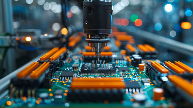
An automatic SMD pick and place machine is a robotic system designed to accurately pick electronic components from feeders and place them onto PCBs with high precision using vision systems and robotic arms. These machines are essential for high-speed, high-volume electronics manufacturing.
2. How does AI improve SMD placement machines?
AI enhances SMD placement machines by optimizing component placement paths, predicting maintenance needs, adapting to new components or PCB designs without extensive reprogramming, and enabling real-time defect detection and correction. This leads to increased accuracy, efficiency, and reduced downtime.
3. What are the challenges faced by modern SMD placement machines?
Modern challenges include handling extremely small components, managing complex and high-density PCB layouts, ensuring flexibility for diverse product lines, and integrating new materials that may have unique handling requirements. These are addressed through modular machine designs, advanced vision systems, and AI-driven control.
4. How are new materials impacting SMD placement technology?
New materials such as graphene composites, ceramic-polymer hybrids, and flexible polyimide substrates improve thermal management, electrical performance, and environmental sustainability. SMD placement machines are evolving to handle these materials delicately and efficiently, expanding the range of possible applications.
5. What future trends will shape SMD placement technology?
Future trends include deeper integration with IoT and smart factory systems, combining pick and place with additive manufacturing for rapid prototyping, increased focus on sustainability, and machines capable of micron-level precision at ultra-high speeds. AI and machine learning will continue to drive automation and process optimization.


