Content Menu
● Understanding SMT Process for PCB
>> Design Phase
>> Printing Solder Paste
>> Placing Components
>> Reflow Soldering
>> Inspection
● Key Benefits of SMT in PCB Manufacturing
>> 1. Increased Component Density
>> 2. Smaller PCB Size
>> 3. Improved Performance
>> 4. Cost-Effectiveness
>> 5. Enhanced Reliability
>> 6. Flexibility in Design
>> 7. Automation and Efficiency
>> 8. Compatibility with Advanced Technologies
>> 9. Environmental Benefits
● Conclusion
● FAQ
>> 1. What is SMT in PCB manufacturing?
>> 2. How does the SMT process improve production efficiency?
>> 3. What are the advantages of using SMT over through-hole technology?
>> 4. Can SMT components be used in high-frequency applications?
>> 5. What environmental benefits does SMT offer?
Surface Mount Technology (SMT) has revolutionized the landscape of printed circuit board (PCB) manufacturing. This innovative technology has become the standard in the electronics industry, offering numerous advantages over traditional through-hole technology. In this article, we will explore the key benefits of using SMT in PCB manufacturing, delving into its processes, applications, and the reasons behind its widespread adoption.

Understanding SMT Process for PCB
The SMT process for PCB involves mounting electronic components directly onto the surface of a printed circuit board. Unlike traditional methods where components are inserted into holes drilled in the PCB, SMT allows for a more compact design and higher component density. The SMT process typically includes several stages: design, printing solder paste, placing components, reflow soldering, and inspection.
Design Phase
The first step in the SMT process is the design phase. Engineers use specialized software to create the PCB layout, ensuring that components are placed efficiently. This phase is crucial as it determines the overall functionality and manufacturability of the PCB. The design must consider factors such as component size, spacing, and the thermal and electrical characteristics of the materials used.
Printing Solder Paste
Once the design is finalized, the next step is to print solder paste onto the PCB. Solder paste is a mixture of tiny solder balls and flux, which helps in the soldering process. A stencil is used to apply the solder paste accurately to the pads where components will be placed. This step is vital as it ensures that the right amount of solder is available for each component, preventing issues such as cold solder joints or excess solder.
Placing Components
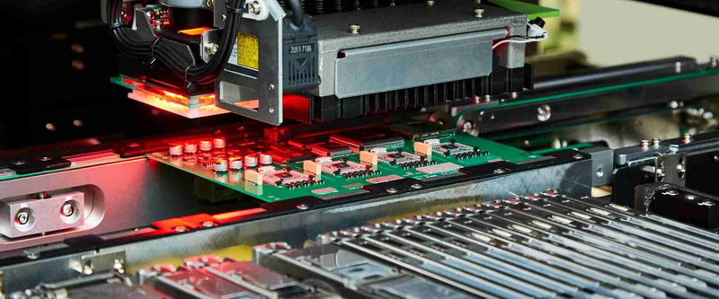
After the solder paste is applied, the components are placed onto the PCB. This is typically done using a pick-and-place machine, which can rapidly and accurately position thousands of components per hour. The ability to place components with high precision is one of the significant advantages of SMT, as it allows for smaller and more complex designs.
Reflow Soldering
Once the components are placed, the PCB undergoes reflow soldering. This process involves heating the PCB in a reflow oven, where the solder paste melts and forms a solid connection between the components and the PCB. The reflow process is carefully controlled to ensure that the solder flows correctly and that components are not damaged by excessive heat.
Inspection
The final stage of the SMT process is inspection. Automated optical inspection (AOI) systems are commonly used to check for defects such as misaligned components, insufficient solder, or solder bridges. This step is crucial for ensuring the quality and reliability of the final product.

Key Benefits of SMT in PCB Manufacturing
The adoption of SMT in PCB manufacturing offers several key benefits that have made it the preferred choice for many electronics manufacturers.
1. Increased Component Density
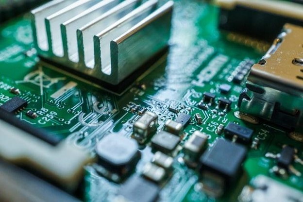
One of the most significant advantages of SMT is the ability to increase component density on PCBs. Since components are mounted on the surface rather than through holes, more components can fit into a smaller area. This is particularly beneficial for modern electronic devices that require compact designs, such as smartphones, tablets, and wearable technology.
2. Smaller PCB Size
With the increased component density comes the ability to produce smaller PCBs. SMT allows for the design of more compact electronic devices, which is essential in today's market where portability is a key factor. Smaller PCBs also lead to lighter products, making them more appealing to consumers.
3. Improved Performance
SMT can enhance the performance of electronic devices. The shorter electrical paths created by surface mounting reduce signal loss and improve overall performance. Additionally, SMT components are often more reliable due to their lower profile and better thermal management, which can lead to longer product lifespans.
4. Cost-Effectiveness
While the initial setup for SMT may be higher due to the need for specialized equipment, the long-term cost savings are significant. SMT allows for faster production rates, reducing labor costs and increasing throughput. Furthermore, the reduced size and weight of SMT components can lead to lower shipping and material costs.
5. Enhanced Reliability
SMT components are generally more reliable than their through-hole counterparts. The solder joints created during the reflow process are typically stronger and less prone to mechanical stress. Additionally, SMT components are less susceptible to damage from vibration and thermal cycling, making them ideal for use in demanding environments.
6. Flexibility in Design
The SMT process allows for greater flexibility in PCB design. Engineers can easily incorporate a wide variety of components, including passive and active devices, into their designs. This flexibility enables the development of innovative products that can meet the ever-changing demands of the electronics market.
7. Automation and Efficiency
The SMT process is highly automated, which leads to increased efficiency in PCB manufacturing. Automated machines can handle multiple tasks, from solder paste application to component placement and inspection. This automation reduces the likelihood of human error and speeds up the production process, allowing manufacturers to meet tight deadlines.
8. Compatibility with Advanced Technologies
SMT is compatible with various advanced technologies, such as mixed-signal and high-frequency applications. This compatibility is essential for modern electronics, which often require the integration of multiple technologies into a single device. SMT allows for the seamless integration of these technologies, enabling the development of sophisticated electronic systems.
9. Environmental Benefits
The SMT process can also offer environmental benefits. The reduction in PCB size and weight leads to less material usage and waste. Additionally, the efficiency of SMT manufacturing processes can result in lower energy consumption, contributing to a more sustainable production environment.
Conclusion
In conclusion, the key benefits of using SMT in PCB manufacturing are numerous and impactful. From increased component density and smaller PCB sizes to improved performance and cost-effectiveness, SMT has transformed the way electronic devices are designed and produced. As technology continues to advance, the importance of SMT in the electronics industry will only grow, making it an essential consideration for manufacturers looking to stay competitive in the market.

FAQ
1. What is SMT in PCB manufacturing?
SMT, or Surface Mount Technology, is a method of mounting electronic components directly onto the surface of a printed circuit board, allowing for higher component density and smaller PCB sizes.
2. How does the SMT process improve production efficiency?
The SMT process improves production efficiency through automation, allowing for faster component placement and reduced labor costs, leading to higher throughput.
3. What are the advantages of using SMT over through-hole technology?
The advantages of SMT over through-hole technology include increased component density, smaller PCB sizes, improved performance, and enhanced reliability.
4. Can SMT components be used in high-frequency applications?
Yes, SMT components are compatible with high-frequency applications, making them suitable for modern electronic devices that require advanced technologies.
5. What environmental benefits does SMT offer?
SMT offers environmental benefits such as reduced material usage, less waste, and lower energy consumption during the manufacturing process.


