Content Menu
● Introduction to Surface Mount Device Packages
>> Importance of SMD Package Types
● Common Types of Surface Mount Device Packages
>> Dual In-line Package (DIP)
>> Small Outline Integrated Circuit (SOIC)
>> Thin Small Outline Package (TSOP)
>> Quad Flat Package (QFP)
>> Ball Grid Array (BGA)
>> Chip-on-Board (COB)
>> Land Grid Array (LGA)
>> Plastic Leaded Chip Carrier (PLCC)
>> Micro Lead Frame Package (MLF)
>> Wafer Level Chip Scale Package (WLCSP)
● Factors Influencing SMD Package Selection
● Advantages and Disadvantages of Various SMD Packages
● Future Trends in Surface Mount Device Packaging
● Conclusion
● Related Questions
>> 1. What is Surface Mount Technology?
>> 2. What are the benefits of using SMD packages over traditional through-hole packages?
>> 3. How do I choose the right SMD package type for my project?
>> 4. What industries commonly use surface mount device packages?
>> 5. Are there any special considerations when soldering SMD packages?
Surface mount technology (SMT) has revolutionized the electronics industry by enabling the miniaturization of devices and improving assembly efficiency. One of the critical components of SMT is the surface mount device (SMD) package. Understanding the various types of surface mount device packages is essential for engineers, designers, and manufacturers in selecting the appropriate package for their applications. This article delves into the different types of surface mount device packages, their characteristics, advantages, and applications.

Introduction to Surface Mount Device Packages
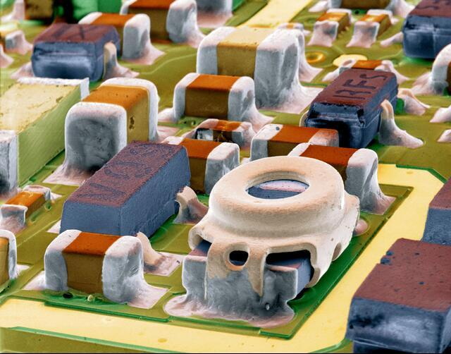
Surface mount devices are electronic components that are mounted directly onto the surface of printed circuit boards (PCBs). Unlike traditional through-hole components, which require holes drilled into the PCB, SMDs allow for a more compact design and higher density of components on a board. The choice of SMD package type can significantly influence the performance, reliability, and manufacturability of electronic products.
Importance of SMD Package Types
The selection of an appropriate SMD package is crucial for several reasons:
- Space Efficiency: Smaller packages allow for more components on a PCB, which is vital for modern compact devices.
- Thermal Management: Different package types have varying thermal characteristics, affecting heat dissipation in high-power applications.
- Electrical Performance: The design and size of a package can influence signal integrity and electromagnetic interference (EMI).
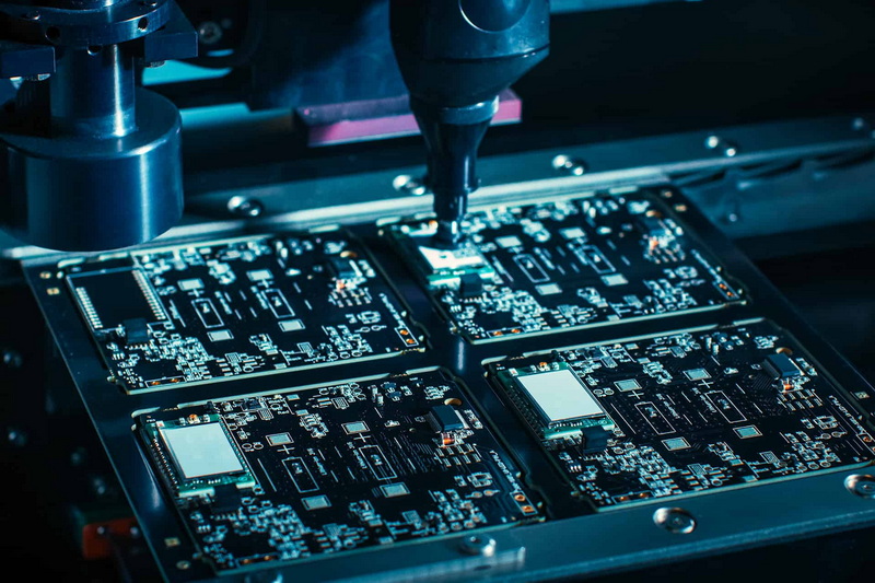
- Manufacturing Process: Some packages are easier to handle during assembly than others, impacting production efficiency.
Common Types of Surface Mount Device Packages
There are several common types of surface mount device packages, each designed for specific applications and requirements.
Dual In-line Package (DIP)
The Dual In-line Package (DIP) is one of the earliest forms of surface mount packaging. It features two parallel rows of pins and is often used for integrated circuits (ICs). While not as compact as other SMD types, DIP packages are still prevalent due to their ease of handling and compatibility with automated assembly processes.
DIPs are often used in applications where space is not critically limited but where reliability and ease of replacement are important. They also allow for easy prototyping since they can be inserted into breadboards or socketed.
Small Outline Integrated Circuit (SOIC)
The Small Outline Integrated Circuit (SOIC) is a popular SMD package that offers a smaller footprint than DIP. SOICs typically have a width ranging from 3 to 12 mm and can contain multiple pins on each side. They are widely used in consumer electronics due to their balance between size and ease of soldering.
SOIC packages provide good thermal performance and are suitable for applications requiring moderate pin counts without occupying excessive PCB space. Their design allows for efficient manufacturing processes, making them a common choice in mass production.
Thin Small Outline Package (TSOP)
The Thin Small Outline Package (TSOP) is an even slimmer version of the SOIC, designed for applications requiring minimal height. TSOPs are commonly used in memory chips like DRAM and flash memory due to their compact design and efficient thermal management properties.
The reduced height makes TSOPs ideal for mobile devices where space is at a premium. However, their thin profile can make them more susceptible to damage during handling and soldering processes.
Quad Flat Package (QFP)
The Quad Flat Package (QFP) features pins on all four sides and is typically used for more complex ICs that require a higher pin count. QFPs can have varying lead pitches, making them suitable for a wide range of applications from microcontrollers to digital signal processors.
QFPs provide excellent electrical performance due to their short lead lengths, which help minimize inductance and improve signal integrity. However, they require precise alignment during assembly due to their larger number of pins compared to other packages.
Ball Grid Array (BGA)
The Ball Grid Array (BGA) is a highly advanced packaging technology that uses an array of solder balls on the bottom side instead of pins. This design allows for excellent thermal performance and electrical connectivity, making BGAs ideal for high-performance applications such as CPUs and GPUs.
BGAs offer several advantages over traditional pin-based packages, including reduced inductance and improved heat dissipation capabilities. However, they can be more challenging to inspect after soldering due to their bottom-mounted solder balls.
Chip-on-Board (COB)
Chip-on-Board (COB) packaging involves directly mounting bare semiconductor chips onto a PCB. This method allows for maximum space savings but requires careful handling during manufacturing due to the fragility of the chips. COB is often used in LED lighting and other applications where space is at a premium.
COB technology can significantly reduce overall package size while enhancing electrical performance by minimizing interconnect lengths between chips and PCBs.
Land Grid Array (LGA)
The Land Grid Array (LGA) is similar to BGA but features flat pads instead of solder balls. This type allows for easy alignment during assembly and provides excellent thermal performance. LGAs are commonly used in high-performance computing applications where heat dissipation is critical.
LGAs also facilitate easier rework since they do not require specialized equipment like BGAs do; however, precise manufacturing techniques are still necessary to ensure reliable connections.

Plastic Leaded Chip Carrier (PLCC)
The Plastic Leaded Chip Carrier (PLCC) has leads extending from all four sides but maintains a square or rectangular shape. PLCCs are often used in programmable logic devices due to their ease of handling during assembly.
PLCC packages offer good mechanical stability while providing sufficient lead length for reliable solder joints on PCBs, making them suitable for various applications in consumer electronics.
Micro Lead Frame Package (MLF)
Micro Lead Frame Packages (MLF) feature very thin leads that provide excellent electrical performance while minimizing space requirements. MLFs are often used in RF applications where size and performance are critical.
MLFs allow designers to achieve high-density layouts without compromising signal integrity or thermal performance, making them ideal for modern communication devices.
Wafer Level Chip Scale Package (WLCSP)
Wafer Level Chip Scale Packages (WLCSP) provide an ultra-compact solution by packaging at the wafer level before dicing into individual chips. This technology reduces package size significantly while maintaining high performance, making it ideal for mobile devices.
WLCSPs offer exceptional electrical performance due to their close proximity to the PCB substrate but may require specialized processing techniques during manufacturing.
Factors Influencing SMD Package Selection
When selecting an SMD package type, several factors must be considered:
- Application Requirements: The specific needs of the application will dictate which package type is most suitable.
- Size Constraints: The physical dimensions available on the PCB will limit the choice of package.
- Thermal Management Needs: High-power applications may require packages with better heat dissipation capabilities.
- Cost Considerations: The price difference between various package types can influence selection based on budget constraints.
- Manufacturing Capabilities: The available technology and processes at manufacturing facilities may also impact which package types can be feasibly produced.
Advantages and Disadvantages of Various SMD Packages
Each type of surface mount device package comes with its own set of advantages and disadvantages:
| Package Type | Advantages | Disadvantages |
| DIP | Easy to handle; cost-effective | Larger footprint; limited pin count |
| SOIC | Compact; good solderability | Limited height; may not fit all designs |
| TSOP | Very thin; efficient thermal management | Fragile; requires careful handling |
| QFP | High pin count; versatile | More complex assembly; larger footprint |
| BGA | Excellent thermal performance; high density | Difficult to inspect; requires specialized equipment |
| COB | Maximum space savings; direct chip attachment | Fragile chips; complex manufacturing |
| LGA | Easy alignment; good thermal performance | Requires precise manufacturing techniques |
| PLCC | Good handling characteristics; versatile | Larger than some alternatives |
| MLF | Excellent electrical performance; compact size | May require specialized assembly techniques |
| WLCSP | Ultra-compact; high performance | Complex manufacturing process |
Future Trends in Surface Mount Device Packaging
As technology advances, we can expect several trends in surface mount device packaging:
- Miniaturization: Continued demand for smaller electronic devices will drive innovations in packaging technologies that allow even greater component density on PCBs.
- Integration: There will be an increased focus on integrating multiple functions within single packages, such as combining analog and digital functions or integrating passive components directly into IC packages.
- Thermal Management Solutions: As devices become more powerful, effective thermal management solutions will become increasingly important in package design.
- Environmentally Friendly Materials: With growing concerns about environmental sustainability, there will likely be a shift towards using eco-friendly materials in packaging processes.
- Advanced Assembly Techniques: Innovations in automated assembly processes will improve efficiency while reducing costs associated with handling complex SMD packages.
Conclusion
Understanding the different types of surface mount device packages is essential for anyone involved in electronics design or manufacturing. Each package type offers unique advantages that can cater to specific application needs while also presenting challenges that must be addressed during design and production phases. By carefully considering factors such as size constraints, thermal management requirements, cost implications, and future trends in technology advancements, engineers can select the most suitable SMD package type for their projects.
As technology continues to evolve, so too will the designs and capabilities of surface mount device packages, paving the way for even more compact and efficient electronic devices in the future.

Related Questions
1. What is Surface Mount Technology?
Surface Mount Technology refers to a method where electronic components are mounted directly onto the surface of PCBs rather than being inserted into holes drilled into them.
2. What are the benefits of using SMD packages over traditional through-hole packages?
SMD packages allow for higher component density on PCBs, reduced manufacturing costs, improved electrical performance, and better thermal management compared to traditional through-hole packages.
3. How do I choose the right SMD package type for my project?
Consider factors such as application requirements, size constraints on your PCB, thermal management needs, and cost when selecting an SMD package type.
4. What industries commonly use surface mount device packages?
Surface mount device packages are widely used across various industries including consumer electronics, telecommunications, automotive electronics, medical devices, and industrial automation.
5. Are there any special considerations when soldering SMD packages?
Yes, soldering SMD packages requires precise techniques such as reflow soldering or wave soldering due to their small size and lead configurations to ensure reliable connections without damaging components.


