Content Menu
● Understanding PCB SMT Assembly
● Common Challenges in PCB SMT Assembly
>> 1. Component Placement Accuracy
>> 2. Solder Paste Application
>> 3. Reflow Soldering Challenges
>> 4. Handling Fine-Pitch Components
>> 5. Warpage and PCB Deformation
● Advanced Techniques to Overcome SMT Assembly Challenges
>> Implementing Automated Optical Inspection (AOI)
>> Utilizing X-ray Inspection for Hidden Defects
>> Implementing Statistical Process Control (SPC)
● Emerging Technologies in PCB SMT Assembly
>> 1. Artificial Intelligence and Machine Learning
>> 2. Industry 4.0 and Smart Factory Integration
>> 3. Advanced Materials and Nano-coatings
● Best Practices for Efficient PCB SMT Assembly
>> 1. Design for Manufacturability (DFM)
>> 2. Comprehensive Training Programs
>> 3. Regular Equipment Maintenance and Calibration
>> 4. Environmental Control
>> 5. Continuous Process Improvement
● Overcoming Specific SMT Assembly Defects
>> 1. Tombstoning
>> 2. Solder Bridging
>> 3. Component Skewing
>> 4. Insufficient Solder Joints
>> 5. Non-Wetting or De-Wetting
● The Future of PCB SMT Assembly
● Conclusion
● FAQ
>> 1. What is PCB SMT service?
>> 2. How does PCB SMT service differ from traditional through-hole assembly?
>> 3. What are the key advantages of using PCB SMT service?
>> 4. What types of components are typically used in PCB SMT service?
>> 5. How can I ensure the quality of PCB SMT service for my project?
● Citations:
Surface Mount Technology (SMT) has revolutionized the electronics manufacturing industry, enabling the production of smaller, more efficient, and highly reliable devices. However, the PCB SMT assembly process comes with its own set of challenges that manufacturers must overcome to ensure high-quality products. This article will explore the common challenges faced in PCB SMT assembly and provide effective solutions to address them.

Understanding PCB SMT Assembly
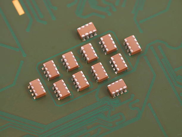
Before delving into the challenges, it's essential to understand what PCB SMT assembly entails. SMT is a method where electronic components are mounted directly onto the surface of a printed circuit board (PCB). This technique has largely replaced the traditional through-hole technology due to its numerous advantages, including higher component density, improved performance, and cost-effectiveness[3].
Common Challenges in PCB SMT Assembly
1. Component Placement Accuracy
One of the most critical challenges in PCB SMT assembly is ensuring accurate placement of components on the PCB. Misaligned components can lead to short circuits, open circuits, or reduced performance of the final product[1].
Solution:
- Invest in high-precision placement machines and regularly calibrate them.
- Provide thorough training to operators on the importance of placement accuracy.
- Implement regular maintenance schedules for equipment to ensure optimal performance[1].
2. Solder Paste Application
Inconsistent or insufficient solder paste application can result in weak solder joints, tombstoning, and bridging issues[1].
Solution:
- Use high-quality stencils specifically designed for your PCB layout.
- Ensure proper alignment of the stencil with the PCB and clean it regularly.
- Implement automated solder paste inspection (SPI) systems to detect defects early in the process[1].
3. Reflow Soldering Challenges
The reflow soldering process is critical in SMT assembly, and issues during this stage can lead to various defects[3].
Solution:
- Optimize the reflow profile for each specific PCB design.
- Use advanced reflow ovens with multiple heating zones for precise temperature control.
- Implement proper cooling strategies to prevent thermal shock to components[3].
4. Handling Fine-Pitch Components
As components become smaller and more densely packed, handling fine-pitch components becomes increasingly challenging[5].
Solution:
- Invest in advanced vision systems and precise equipment capable of handling ultra-small components.
- Implement stringent process controls throughout the assembly process.
- Consider using nano-coated stencils to improve solder paste release for fine-pitch applications[5].
5. Warpage and PCB Deformation
PCB warpage during the assembly process can cause misalignments and poor solder joints, especially for large or thin boards[1].
Solution:
- Use support fixtures during the assembly process to minimize board warpage.
- Optimize the PCB design to reduce the risk of warpage.
- Implement proper storage and handling procedures for PCBs to prevent moisture absorption[1].
Advanced Techniques to Overcome SMT Assembly Challenges
Implementing Automated Optical Inspection (AOI)
AOI systems play a crucial role in detecting defects early in the assembly process. These systems use high-resolution cameras and advanced image processing algorithms to identify issues such as component misalignment, solder bridging, and missing components[3].
Benefits of AOI:
- Rapid inspection of large numbers of PCBs
- Consistent and objective defect detection
- Ability to detect defects that may be missed by human inspectors
Utilizing X-ray Inspection for Hidden Defects
X-ray inspection is particularly useful for detecting hidden defects in complex PCB assemblies, especially those with ball grid array (BGA) components or dense multi-layer boards[10].
Advantages of X-ray Inspection:
- Non-destructive testing method
- Ability to detect voids in solder joints
- Inspection of hidden solder joints beneath components
Implementing Statistical Process Control (SPC)
SPC involves using statistical methods to monitor and control the SMT assembly process. By collecting and analyzing data from various stages of the assembly process, manufacturers can identify trends and potential issues before they lead to defects[10].
Benefits of SPC:
- Early detection of process drift
- Continuous improvement of assembly processes
- Reduction in defect rates and rework costs
Emerging Technologies in PCB SMT Assembly
1. Artificial Intelligence and Machine Learning
AI and machine learning algorithms are being increasingly used to optimize SMT assembly processes. These technologies can analyze vast amounts of data from various sensors and inspection systems to predict potential defects and suggest process improvements[10].
Applications of AI in SMT Assembly:
- Predictive maintenance of assembly equipment
- Optimization of component placement and reflow profiles
- Enhanced defect detection and classification
2. Industry 4.0 and Smart Factory Integration
The concept of Industry 4.0 and smart factories is transforming PCB SMT assembly. By integrating various systems and processes, manufacturers can achieve higher levels of automation, efficiency, and quality control[10].
Key Features of Smart SMT Assembly:
- Real-time monitoring and control of assembly processes
- Seamless integration of design, production, and quality control systems
- Enhanced traceability and data-driven decision making
3. Advanced Materials and Nano-coatings
The development of new materials and nano-coatings is addressing some of the challenges in SMT assembly. For example, nano-coated stencils can improve solder paste release and reduce the risk of defects in fine-pitch applications[5].
Benefits of Advanced Materials:
- Improved solder joint reliability
- Enhanced thermal management
- Reduced risk of component failure due to environmental factors

Best Practices for Efficient PCB SMT Assembly
1. Design for Manufacturability (DFM)
Implementing DFM principles from the early stages of PCB design can significantly reduce assembly challenges and improve overall product quality[9].
Key DFM Considerations:
- Optimizing component placement for efficient assembly
- Ensuring adequate spacing between components
- Designing for proper thermal management
2. Comprehensive Training Programs
Investing in comprehensive training programs for assembly operators and technicians is crucial for maintaining high-quality standards in SMT assembly[1].
Training Focus Areas:
- Proper handling of components and PCBs
- Understanding and troubleshooting common assembly issues
- Effective use of inspection and quality control equipment
3. Regular Equipment Maintenance and Calibration
Implementing a rigorous maintenance and calibration schedule for all SMT assembly equipment is essential for consistent performance and quality[1].
Maintenance Best Practices:
- Regular cleaning and lubrication of moving parts
- Calibration of placement machines and inspection systems
- Proactive replacement of wear parts
4. Environmental Control
Maintaining proper environmental conditions in the assembly area is crucial for preventing issues related to static electricity, humidity, and temperature fluctuations[3].
Environmental Control Measures:
- Implementation of electrostatic discharge (ESD) protection measures
- Humidity and temperature control in storage and assembly areas
- Use of clean room practices for sensitive assemblies
5. Continuous Process Improvement
Implementing a culture of continuous improvement is essential for addressing evolving challenges in PCB SMT assembly[10].
Continuous Improvement Strategies:
- Regular review and analysis of defect data
- Encouraging feedback and suggestions from assembly operators
- Staying updated with the latest industry trends and technologies
Overcoming Specific SMT Assembly Defects
1. Tombstoning
Tombstoning occurs when a component lifts on one end during reflow soldering, resembling a tombstone[9].
Prevention Strategies:
- Ensure balanced solder paste deposition on both pads
- Optimize pad design and component placement
- Adjust reflow profile to prevent uneven heating
2. Solder Bridging
Solder bridging is the formation of unwanted connections between adjacent solder joints[1].
Prevention Strategies:
- Optimize stencil design and aperture size
- Ensure proper solder paste viscosity and metal content
- Implement proper reflow profiling to prevent solder paste slump
3. Component Skewing
Component skewing occurs when components are misaligned during placement or reflow[9].
Prevention Strategies:
- Ensure accurate component placement
- Optimize pad design for self-alignment during reflow
- Implement proper handling and storage of components to prevent warpage
4. Insufficient Solder Joints
Insufficient solder joints can lead to weak connections and potential circuit failures[9].
Prevention Strategies:
- Optimize stencil thickness and aperture design
- Ensure proper solder paste volume and viscosity
- Implement effective solder paste inspection (SPI) procedures
5. Non-Wetting or De-Wetting
Non-wetting or de-wetting occurs when solder fails to properly adhere to component leads or PCB pads[9].
Prevention Strategies:
- Ensure proper PCB surface finish and cleanliness
- Optimize reflow profile to activate flux properly
- Use high-quality solder paste with appropriate flux content
The Future of PCB SMT Assembly
As technology continues to advance, the future of PCB SMT assembly looks promising. We can expect to see further miniaturization of components, increased automation, and the integration of advanced technologies such as AI and machine learning. These advancements will help address current challenges and open up new possibilities for electronic device design and manufacturing.
Some key trends to watch in the future of PCB SMT assembly include:
1. Increased use of 3D printing technologies for rapid prototyping and small-scale production of PCBs and components.
2. Development of new solder materials that offer improved reliability and environmental friendliness.
3. Integration of augmented reality (AR) technologies for assembly guidance and quality control.
4. Advanced thermal management solutions to address the challenges of high-density, high-power PCB designs.
5. Increased focus on sustainability in PCB manufacturing and assembly processes.
Conclusion
PCB SMT assembly, while offering numerous advantages, comes with its own set of challenges. By understanding these challenges and implementing effective solutions, manufacturers can significantly improve their assembly processes, reduce defects, and produce high-quality electronic products. The key to success lies in a combination of advanced technologies, proper training, stringent quality control measures, and a commitment to continuous improvement.
As the electronics industry continues to evolve, PCB SMT assembly will play an increasingly crucial role in enabling the development of smaller, more powerful, and more reliable electronic devices. By staying abreast of the latest technologies and best practices, manufacturers can ensure they remain competitive in this rapidly changing landscape.

FAQ
1. What is PCB SMT service?
PCB SMT service refers to the process of assembling electronic components onto printed circuit boards using Surface Mount Technology. This service includes component placement, solder paste application, reflow soldering, and quality inspection. PCB SMT service providers offer expertise and specialized equipment to efficiently produce high-quality PCB assemblies for various electronic applications[3][7].
2. How does PCB SMT service differ from traditional through-hole assembly?
PCB SMT service utilizes surface-mounted components that are soldered directly onto the PCB surface, while through-hole assembly involves components with leads inserted through holes in the PCB. SMT allows for higher component density, smaller board sizes, and often faster and more automated assembly processes compared to through-hole technology[3][7].
3. What are the key advantages of using PCB SMT service?
The main advantages of PCB SMT service include:
- Higher component density and smaller board sizes
- Improved electrical performance due to shorter connection paths
- Faster and more automated assembly processes
- Better mechanical performance in shock and vibration environments
- Lower production costs for high-volume manufacturing[3][5][7]
4. What types of components are typically used in PCB SMT service?
Common components used in PCB SMT service include:
- Resistors and capacitors in various package sizes (e.g., 0201, 0402, 0603)
- Integrated circuits in packages like QFP, BGA, and CSP
- LEDs and other optoelectronic components
- Inductors and transformers
- Connectors designed for surface mounting[3][7]
5. How can I ensure the quality of PCB SMT service for my project?
To ensure high-quality PCB SMT service:
- Choose a reputable service provider with experience in your industry
- Provide clear and detailed design specifications
- Implement Design for Manufacturability (DFM) principles
- Request prototypes or small production runs before full-scale manufacturing
- Utilize advanced inspection techniques like AOI and X-ray inspection
- Maintain open communication with your service provider throughout the process[1][3][9]
Citations:
[1] https://www.bigmateph.com/what-are-the-common-challenges-of-smt-and-how-to-overcome-it/
[2] https://www.macdermidalpha.com/sites/default/files/2021-09/ALPHA%20SMT%20Troubleshooting%20Guide%20EN%2001Jun20%20BR_0.pdf
[3] https://www.pcbonline.com/blog/pcb-assembly-services.html
[4] https://www.viasion.com/blog/common-challenges-in-smt-assembly-and-solutions/
[5] https://www.pcbjhy.com/blog/pros-and-cons-of-smt-pcb-assembly/
[6] https://www.bestproto.net/news/common-challenges-in-pcb-assembly-and-how-to-overcome-them/
[7] https://versae.com/smt-assembly-faq/
[8] https://smtnet.com/library/index.cfm?fuseaction=browse_articles&start_at=296
[9] https://jhdpcb.com/blog/efficient-smt-assembly/
[10] https://pmc.ncbi.nlm.nih.gov/articles/PMC9228397/
[11] https://www.protoexpress.com/blog/common-errors-surface-mount-technology-smt/


