Content Menu
● Introduction
● Understanding PCB SMT Terminals
● How PCB SMT Terminals Work
● Types of PCB SMT Terminals
>> 1. Header Connectors
>> 2. Socket Connectors
>> 3. Terminal Blocks
>> 4. Card Edge Connectors
>> 5. FPC/FFC Connectors
● Advantages of PCB SMT Terminals
● Applications of PCB SMT Terminals
>> Consumer Electronics
>> Automotive Electronics
>> Industrial Control Systems
>> Telecommunications
>> Medical Devices
● Design Considerations for PCB SMT Terminals
● Best Practices for PCB SMT Terminal Assembly
● Challenges and Solutions in PCB SMT Terminal Implementation
>> Challenge 1: Solder Joint Reliability
>> Challenge 2: Thermal Management
>> Challenge 3: Signal Integrity
>> Challenge 4: Rework and Repair
>> Challenge 5: Moisture Sensitivity
● Future Trends in PCB SMT Terminal Technology
● Conclusion
● Frequently Asked Questions (FAQ)
>> 1. What are the main differences between SMT and through-hole terminals?
>> 2. How do I choose the right PCB SMT terminal for my application?
>> 3. What are some common issues encountered with PCB SMT terminals, and how can they be prevented?
>> 4. Can PCB SMT terminals be used in high-temperature environments?
>> 5. How does the use of PCB SMT terminals impact the overall cost of electronics manufacturing?
● Citations:
Introduction
In the ever-evolving world of electronics manufacturing, Surface Mount Technology (SMT) has revolutionized the way components are attached to Printed Circuit Boards (PCBs). Among these components, PCB SMT terminals play a crucial role in establishing electrical connections and facilitating signal transmission. This article delves into the intricacies of PCB SMT terminals, exploring their functionality, types, advantages, and applications in modern electronics.

Understanding PCB SMT Terminals
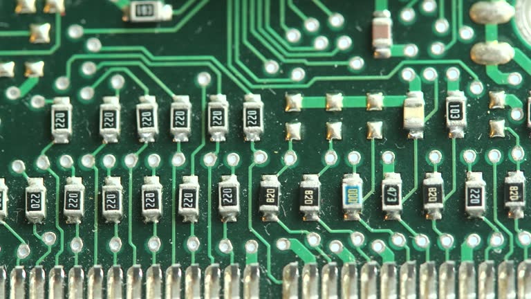
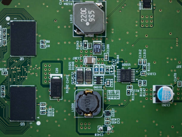
PCB SMT terminals, also known as surface mount terminals or SMT connectors, are specialized electronic components designed to create reliable electrical connections on PCBs using surface mount technology. Unlike traditional through-hole terminals, SMT terminals are mounted directly onto the surface of the PCB, eliminating the need for drilled holes[1].
These terminals serve as interface points between the PCB and external devices or other circuit boards. They come in various shapes, sizes, and configurations to accommodate different electrical and mechanical requirements. PCB SMT terminals are essential in creating compact, efficient, and cost-effective electronic assemblies across a wide range of industries.
How PCB SMT Terminals Work
The functionality of PCB SMT terminals is based on the principles of surface mount technology. Here's a step-by-step explanation of how these terminals work:
1. Solder Paste Application: The process begins with the application of solder paste to specific areas on the PCB where the terminals will be placed. This is typically done using a stencil printer, which applies a precise amount of solder paste to the designated pads[7].
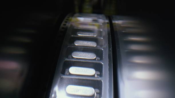
2. Terminal Placement: Using automated pick-and-place machines, the SMT terminals are accurately positioned onto the solder paste-covered pads on the PCB. The machines use vacuum nozzles and high-precision cameras to ensure correct placement[3].
3. Reflow Soldering: Once all components, including the SMT terminals, are placed, the PCB undergoes reflow soldering. In this process, the board is passed through a reflow oven where it is subjected to a carefully controlled temperature profile. The heat causes the solder paste to melt and form secure electrical and mechanical connections between the terminals and the PCB[7].
4. Cooling and Solidification: As the PCB cools, the solder solidifies, creating permanent connections between the SMT terminals and the board. This process ensures a robust and reliable electrical interface[3].
5. Inspection and Testing: After the reflow process, the PCB undergoes visual inspection and electrical testing to verify the quality of the connections and overall functionality of the assembly[7].
Types of PCB SMT Terminals
There are several types of PCB SMT terminals available, each designed for specific applications and requirements. Some common types include:
1. Header Connectors
Header connectors are versatile SMT terminals that come in various pin configurations, such as single-row, dual-row, or matrix arrangements. They are commonly used for board-to-board connections and can accommodate different pitch sizes.
2. Socket Connectors
Socket connectors are the female counterparts to header connectors. They provide a receptacle for mating with pins or headers, allowing for easy connection and disconnection of components or modules.
3. Terminal Blocks
SMT terminal blocks offer a convenient way to connect external wires to a PCB. They typically feature screw terminals or spring-loaded mechanisms for secure wire attachment.
4. Card Edge Connectors
These specialized SMT connectors are designed to accept the edge of a PCB or expansion card. They are commonly used in computer motherboards and other modular electronic systems.
5. FPC/FFC Connectors
Flexible Printed Circuit (FPC) and Flexible Flat Cable (FFC) connectors are SMT terminals designed to interface with flexible circuits or flat cables. They are widely used in compact electronic devices where space is at a premium.
Advantages of PCB SMT Terminals
The use of PCB SMT terminals offers several advantages over traditional through-hole terminals:
1. Compact Design: SMT terminals allow for higher component density on PCBs, enabling the creation of smaller and more compact electronic devices[1].
2. Improved Electrical Performance: The shorter leads and reduced parasitic capacitance of SMT terminals result in better high-frequency performance and signal integrity[3].
3. Cost-Effective Manufacturing: SMT assembly processes are highly automated, reducing labor costs and increasing production efficiency[3].
4. Enhanced Reliability: The direct surface mounting of terminals reduces the risk of mechanical stress on the PCB, leading to improved long-term reliability[1].
5. Design Flexibility: SMT terminals offer greater flexibility in PCB layout and component placement, allowing for more optimized designs[3].

Applications of PCB SMT Terminals
PCB SMT terminals find applications across a wide range of industries and electronic devices:
Consumer Electronics
Smartphones, tablets, laptops, and wearable devices extensively use SMT terminals for various connections, including battery interfaces, display connectors, and sensor modules[3].
Automotive Electronics
Modern vehicles incorporate numerous electronic control units (ECUs) that rely on SMT terminals for reliable connections in challenging automotive environments[3].
Industrial Control Systems
SMT terminals are crucial in industrial automation equipment, process control systems, and robotics, where compact and reliable connections are essential[3].
Telecommunications
High-frequency communication devices, such as routers, switches, and base stations, benefit from the improved signal integrity offered by SMT terminals[3].
Medical Devices
Portable medical equipment, patient monitoring systems, and diagnostic devices utilize SMT terminals to achieve compact and reliable designs[3].
Design Considerations for PCB SMT Terminals
When incorporating PCB SMT terminals into a design, several factors should be considered:
1. Electrical Requirements: Consider the voltage, current, and signal characteristics required for the application when selecting SMT terminals.
2. Mechanical Stress: Evaluate the potential mechanical stresses that the terminals may experience during assembly and in the final product.
3. Environmental Factors: Consider the operating environment, including temperature range, humidity, and exposure to contaminants.
4. PCB Layout: Optimize the PCB layout to accommodate the SMT terminals, ensuring proper spacing and thermal management.
5. Manufacturing Process: Consider the assembly process, including solder paste application, component placement, and reflow soldering parameters.
Best Practices for PCB SMT Terminal Assembly
To ensure successful integration of PCB SMT terminals, follow these best practices:
1. Proper Solder Paste Application: Use high-quality solder paste and ensure accurate stencil design for optimal solder paste deposition[7].
2. Component Placement Accuracy: Utilize advanced pick-and-place machines with vision systems to ensure precise positioning of SMT terminals[3].
3. Reflow Profile Optimization: Develop and maintain an optimized reflow soldering profile that suits the specific SMT terminals and other components on the PCB[7].
4. Cleanliness and Handling: Maintain a clean manufacturing environment and handle PCBs and components with care to prevent contamination and damage[7].
5. Inspection and Testing: Implement thorough visual inspection and electrical testing procedures to verify the quality of SMT terminal connections[7].
Challenges and Solutions in PCB SMT Terminal Implementation
While PCB SMT terminals offer numerous advantages, there are some challenges associated with their implementation:
Challenge 1: Solder Joint Reliability
SMT terminals rely on small solder joints for both electrical and mechanical connections. Ensuring the long-term reliability of these joints can be challenging, especially in high-stress environments.
Solution: Implement proper PCB design practices, such as using appropriate pad sizes and thermal relief patterns. Additionally, consider using lead-free solder alloys with improved mechanical properties and employ X-ray inspection for critical connections.
Challenge 2: Thermal Management
The compact nature of SMT assemblies can lead to heat dissipation issues, potentially affecting the performance and lifespan of SMT terminals.
Solution: Incorporate thermal management techniques such as heat sinks, thermal vias, and proper component spacing. Consider using thermally enhanced SMT terminals for high-power applications.
Challenge 3: Signal Integrity
As operating frequencies increase, maintaining signal integrity becomes more challenging, especially for high-speed SMT terminals.
Solution: Employ proper PCB layout techniques, such as controlled impedance routing and minimizing signal path lengths. Use high-frequency SMT terminals designed for optimal signal performance.
Challenge 4: Rework and Repair
Reworking or replacing SMT terminals can be more challenging compared to through-hole components, potentially leading to increased repair costs.
Solution: Invest in specialized SMT rework equipment and train technicians in proper rework techniques. Consider using modular designs that allow for easier component replacement when feasible.
Challenge 5: Moisture Sensitivity
Some SMT terminals, particularly those with plastic housings, can be sensitive to moisture absorption, potentially leading to issues during reflow soldering.
Solution: Implement proper moisture management procedures, including the use of dry storage and baking processes when necessary. Select moisture-resistant SMT terminals for critical applications.
Future Trends in PCB SMT Terminal Technology
As electronics continue to evolve, PCB SMT terminal technology is also advancing to meet new challenges and requirements:
1. Miniaturization: The trend towards smaller and more compact electronic devices is driving the development of ultra-miniature SMT terminals with even finer pitches and reduced footprints.
2. High-Speed Data Transmission: With the increasing demand for high-speed data transfer, SMT terminals are being designed to support higher frequencies and improved signal integrity for applications such as 5G and beyond.
3. Improved Thermal Performance: As power densities increase, SMT terminals with enhanced thermal management capabilities are being developed to handle higher currents and dissipate heat more effectively.
4. Environmental Sustainability: The electronics industry is moving towards more environmentally friendly materials and processes. This trend is reflected in the development of lead-free and halogen-free SMT terminals.
5. Smart Connectivity: The rise of the Internet of Things (IoT) is driving the development of SMT terminals with integrated intelligence, such as built-in sensors or communication capabilities.
Conclusion
PCB SMT terminals have become an integral part of modern electronics manufacturing, offering numerous advantages in terms of miniaturization, performance, and cost-effectiveness. As we've explored in this article, these components play a crucial role in establishing reliable electrical connections on PCBs across a wide range of applications.
Understanding the functionality, types, and best practices associated with PCB SMT terminals is essential for electronics designers and manufacturers looking to create high-quality, compact, and efficient electronic devices. As technology continues to advance, we can expect further innovations in SMT terminal design, addressing challenges and opening up new possibilities for electronic product development.
By staying informed about the latest developments in PCB SMT terminal technology and adhering to best practices in design and assembly, engineers and manufacturers can leverage these components to create cutting-edge electronic products that meet the demands of an increasingly connected and miniaturized world.

Frequently Asked Questions (FAQ)
1. What are the main differences between SMT and through-hole terminals?
SMT terminals are mounted directly on the PCB surface, while through-hole terminals require holes drilled through the board. SMT terminals allow for higher component density, improved electrical performance, and more efficient automated assembly. Through-hole terminals offer stronger mechanical connections and are better suited for high-power or high-stress applications.
2. How do I choose the right PCB SMT terminal for my application?
When selecting PCB SMT terminals, consider factors such as electrical requirements (voltage, current, frequency), mechanical stress, environmental conditions, PCB space constraints, and manufacturing processes. Consult with terminal manufacturers and refer to datasheets to ensure the chosen terminal meets your specific needs.
3. What are some common issues encountered with PCB SMT terminals, and how can they be prevented?
Common issues include solder joint failures, misalignment during placement, and damage from thermal stress. These can be prevented by using proper PCB design techniques, optimizing the reflow soldering process, implementing thorough inspection procedures, and selecting terminals appropriate for the application's environmental and mechanical requirements.
4. Can PCB SMT terminals be used in high-temperature environments?
Yes, there are high-temperature SMT terminals designed for use in harsh environments. These terminals often use specialized materials and construction techniques to withstand elevated temperatures. When selecting terminals for high-temperature applications, carefully review the manufacturer's specifications and consider factors such as maximum operating temperature and thermal cycling capabilities.
5. How does the use of PCB SMT terminals impact the overall cost of electronics manufacturing?
While SMT terminals may have a higher initial cost compared to some through-hole alternatives, they often lead to overall cost savings in electronics manufacturing. This is due to increased automation in the assembly process, reduced PCB size, improved production efficiency, and potentially lower rework rates. However, the exact cost impact depends on factors such as production volume, terminal complexity, and specific manufacturing processes.
Citations:
[1] https://promaxpogopin.com/professional/smt-connectors-in-pcb-everything-you-need-to-know/
[2] https://patents.google.com/patent/CN112040669B/zh
[3] https://www.wevolver.com/article/what-is-smt
[4] https://patents.google.com/patent/CN108012450A/zh
[5] https://en.wikipedia.org/wiki/Surface-mount_technology
[6] https://patents.google.com/patent/WO2011025507A1/sv
[7] https://www.pcbcart.com/article/content/smt-process-to-cost-reduction.html
[8] https://www.made-in-china.com/products-search/hot-china-products/Smt_Pcb_Connector.html


