Content Menu
● Understanding SMT Stencils
>> Characteristics of SMT Stencils:
● Preparing for Solder Paste Application
>> 1. Gather Necessary Tools and Materials:
>> 2. Warm Up the Solder Paste:
>> 3. Inspect the PCB and Stencil:
● Step-by-Step Guide to Using SMT Stencils
>> Step 1: Secure the PCB
>> Step 2: Align the Stencil
>> Step 3: Apply Solder Paste
>> Step 4: Remove the Stencil
>> Step 5: Inspect for Quality
● Post-Application Steps
● Maintenance of SMT Stencils
● Troubleshooting Common Issues with SMT Stencils
>> Insufficient Solder Paste Deposition
>> Excessive Solder Paste Deposition
>> Bridging or Solder Balling
● Best Practices for Using SMT Stencils
● Advanced Techniques in Using SMT Stencils
>> Automated Printing Machines
>> Multi-Level Stenciling
● Solder Paste Types and Their Implications
>> 1. Lead-Based vs. Lead-Free Pastes:
>> 2. No-Clean vs. Water-Soluble Pastes:
>> 3. Specialty Pastes:
● Environmental Considerations in SMT Processes
● Conclusion
● FAQ
>> 1. What materials are commonly used for SMT stencils?
>> 2. How do I know if my stencil is clogged?
>> 3. What is the optimal thickness for an SMT stencil?
>> 4. How often should I clean my SMT stencil?
>> 5. Can I use an SMT stencil for different types of PCBs?
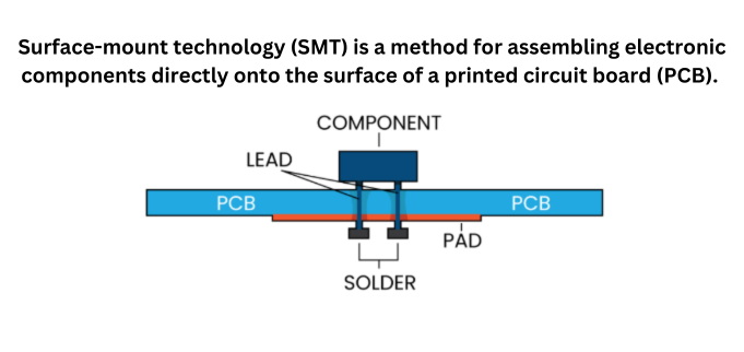
Surface Mount Technology (SMT) has transformed the electronics manufacturing landscape, allowing for the production of smaller, more efficient, and cost-effective printed circuit boards (PCBs). A critical component of this process is the SMT stencil, which facilitates the precise application of solder paste onto PCB pads. This article will provide a comprehensive guide on how to effectively use SMT stencils, covering everything from preparation to application and maintenance.

Understanding SMT Stencils
SMT stencils are thin sheets, typically made from stainless steel or nickel alloys, with laser-cut apertures that correspond to the solder pad locations on a PCB. They are designed to ensure accurate deposition of solder paste, which is essential for creating reliable solder joints between components and the PCB.
Characteristics of SMT Stencils:
- Material: Usually made from stainless steel or Mylar.
- Aperture Design: The size and shape of the stencil apertures determine the volume and precision of solder paste deposition.
- Framed vs. Frameless: Framed stencils are ready to use and provide tension, while frameless stencils require additional setups.
Preparing for Solder Paste Application
Before applying solder paste using an SMT stencil, several preparatory steps must be taken to ensure success:
1. Gather Necessary Tools and Materials:
- SMT stencil
- Printed Circuit Board (PCB)
- Solder paste
- Squeegee or application tool
- PCB holders (to secure the PCB)
- Cleaning supplies (e.g., isopropyl alcohol)
2. Warm Up the Solder Paste:
- Remove solder paste from refrigeration and allow it to reach room temperature. This ensures better flow and adherence during application.
3. Inspect the PCB and Stencil:
- Check that the PCB is clean and free of debris.
- Ensure that the stencil matches the PCB layout and that there are no clogs in the apertures.
Step-by-Step Guide to Using SMT Stencils
Step 1: Secure the PCB
Start by securing your PCB onto a flat surface. If you don't have pre-cut holders, you can use other PCBs of similar thickness to stabilize it. This step is crucial for maintaining alignment during the solder paste application.
Step 2: Align the Stencil
Carefully align the stencil over the PCB, ensuring that each aperture corresponds perfectly with its respective pad on the board. It's recommended to tape only two sides of the stencil to avoid flexing while applying solder paste.
Step 3: Apply Solder Paste
Using a squeegee or an application tool, place a small amount of solder paste at one end of the stencil.
- Technique: Hold the squeegee at a 45-degree angle and gently scrape across the stencil from one side to another. This action should fill each aperture with solder paste without excessive pressure that could cause paste overflow.
- Tip: Make only one pass with the squeegee for best results; multiple passes can lead to uneven deposits.
Step 4: Remove the Stencil
After applying solder paste, carefully lift one side of the stencil while keeping your other hand in place to prevent it from shifting. This should be done in a smooth motion to avoid smudging any solder paste.
Step 5: Inspect for Quality
Once you've removed the stencil, inspect each pad on the PCB to ensure that they are adequately covered with solder paste. If any apertures appear clogged or improperly filled, you may need to clean and reapply.
Post-Application Steps
After successfully applying solder paste using an SMT stencil, follow these steps:
1. Place Components:
- Position your electronic components onto their respective pads while the solder paste is still tacky.
2. Reflow Process:
- Use a reflow oven or hot air station to melt the solder paste, creating strong connections between components and pads.
3. Clean Up:
- Clean your tools and workspace thoroughly after completing your work session. Ensure that any leftover solder paste is disposed of properly.
Maintenance of SMT Stencils
Proper maintenance is essential for prolonging the life of your SMT stencils and ensuring consistent print quality:
- Regular Cleaning: Clean your stencil after each use to remove any residual solder paste that could clog apertures.
- Inspection: Regularly check for damage or wear and tear on both sides of the stencil under good lighting conditions.
- Storage: Store stencils flat in a clean environment to prevent warping or damage during handling.

Troubleshooting Common Issues with SMT Stencils
Despite best efforts, problems can still arise during the stencil printing process. Here are some common issues along with their potential solutions:
Insufficient Solder Paste Deposition
This issue can occur due to clogged apertures or insufficient pressure during application.
- Solutions:
- Increase stencil thickness.
- Enlarge aperture size.
- Increase squeegee pressure.
- Reduce print speed.
- Regularly check for clogged apertures.
Excessive Solder Paste Deposition
Too much solder paste can lead to bridging or excess build-up on pads.
- Solutions:
- Decrease stencil thickness.
- Reduce aperture size.
- Decrease squeegee pressure.
- Increase print speed.
- Inspect for damaged aperture walls.
Bridging or Solder Balling
This occurs when excess solder creates unintended connections between pads.
- Solutions:
- Reduce solder paste volume.
- Increase aperture wall tapering.
- Optimize print parameters.
- Improve cleaning routines for stencils.
Best Practices for Using SMT Stencils
To maximize performance and longevity when using SMT stencils, consider these best practices:
- Choose Appropriate Solder Paste: The type of solder paste used can significantly impact printing quality. Ensure you select one compatible with your stencil material and PCB surface finish.
- Maintain Consistent Pressure: When applying solder paste with a squeegee, maintain even pressure across its length for uniform coverage.
- Use Proper Lighting: A well-lit workspace helps in accurately inspecting both stencils and PCBs during setup and post-printing checks.
- Regular Training: Ensure that all operators are trained in proper techniques for using SMT stencils effectively. Regular workshops can help reinforce best practices.
Advanced Techniques in Using SMT Stencils
For those looking to enhance their skills further, several advanced techniques can be employed:
Automated Printing Machines
Automated printing machines provide higher precision and speed compared to manual methods. They often come equipped with features such as:
- Vision Systems: These systems ensure accurate alignment between stencils and PCBs by using cameras that detect misalignments before printing begins.
- Programmable Settings: Operators can customize parameters such as squeegee speed and pressure based on specific project requirements.
Using automated machines can significantly reduce human error while increasing throughput in high-volume manufacturing environments.
Multi-Level Stenciling
For complex PCBs featuring components at different heights, multi-level stenciling allows manufacturers to apply varying amounts of solder paste based on component requirements. This technique involves:
- Designing multiple stencils for different component heights.
- Utilizing a system that can switch between these stencils as needed during production runs.
This method ensures optimal performance across all components while reducing waste associated with excess solder paste application.
Solder Paste Types and Their Implications
Choosing the right type of solder paste is crucial for achieving desired results in PCB assembly:
1. Lead-Based vs. Lead-Free Pastes:
- Lead-based pastes are known for their excellent wetting properties but are increasingly being phased out due to environmental regulations.
- Lead-free pastes often require higher temperatures during reflow but offer better compliance with RoHS standards.
2. No-Clean vs. Water-Soluble Pastes:
- No-clean pastes leave minimal residues that do not require cleaning after reflow but may not be suitable for all applications.
- Water-soluble pastes require thorough cleaning post-soldering but offer better performance in terms of joint reliability when cleaned properly.
3. Specialty Pastes:
- Specialty pastes designed for specific applications (e.g., high-temperature environments) can enhance performance but may come at a higher cost.
Understanding these differences allows manufacturers to select appropriate materials based on their specific needs and regulatory requirements.
Environmental Considerations in SMT Processes
As electronic manufacturing evolves, environmental considerations have become increasingly important:
- Moisture Sensitivity: Many components used in SMT processes are sensitive to moisture absorption which can lead to defects during reflow processes (known as popcorn effect). Proper storage conditions should be maintained using moisture barrier bags or desiccants until assembly occurs.
- Waste Management: Proper disposal methods must be followed for leftover materials including unused solder paste and defective PCBs containing hazardous materials like lead or cadmium. Implementing recycling programs helps minimize environmental impact while adhering to regulations set forth by governing bodies like EPA or local authorities.
Conclusion
Using SMT stencils effectively can significantly enhance your PCB assembly process by ensuring precise and consistent application of solder paste. By following proper preparation, application techniques, troubleshooting methods, maintenance routines, advanced techniques, understanding material choices, and considering environmental impacts, you can achieve high-quality results in your electronic projects.
This guide serves as a comprehensive resource for both beginners and experienced users looking to refine their skills in using SMT stencils effectively. With attention to detail in every step—from preparation through inspection—you can ensure optimal performance in your electronic assemblies while contributing positively towards sustainable practices within electronics manufacturing industries today.

FAQ
1. What materials are commonly used for SMT stencils?
SMT stencils are typically made from stainless steel or Mylar due to their durability and ability to maintain precision during multiple uses.
2. How do I know if my stencil is clogged?
You can check for clogs by inspecting each aperture visually under good lighting conditions. If you see any residue or if solder paste does not flow through easily, it may be clogged.
3. What is the optimal thickness for an SMT stencil?
The optimal thickness generally ranges from 0.10mm to 0.30mm; however, this can vary based on component size and specific application requirements.
4. How often should I clean my SMT stencil?
It is advisable to clean your stencil after every use or after every few prints if you notice a decline in print quality.
5. Can I use an SMT stencil for different types of PCBs?
Yes, but ensure that each stencil matches its corresponding PCB layout precisely for optimal results in solder paste application.


