Content Menu
● Understanding SMT PCB Assembly
>> What is SMT?
>> Advantages of SMT
● Tools and Materials Needed for SMT PCB Assembly
>> Essential Tools
>> Materials Required
● The SMT PCB Assembly Process
>> Step 1: Design the PCB
>> Step 2: Material Preparation
>> Step 3: Print Solder Paste
>> Step 4: Place Components
>> Step 5: Reflow Soldering
>> Step 6: Cleaning
>> Step 7: Inspection
>> Step 8: Testing
● Common Challenges in SMT Assembly
>> Solder Bridging
>> Insufficient Solder Joints
>> Tombstoning
>> Non-Wetting or De-Wetting
>> Solder Balling
● Solutions to Common Challenges
● Best Practices for SMT PCB Assembly
>> Design Considerations
>> Solder Paste Application
>> Component Placement
>> Reflow Profile Optimization
● Conclusion
● FAQ
>> 1. What is the difference between SMT and through-hole technology?
>> 2. What materials are required for SMT assembly?
>> 3. How does reflow soldering work?
>> 4. What are common defects in SMT assembly?
>> 5. Can I perform SMT assembly at home?
● Citations:
Surface Mount Technology (SMT) is a method used to create electronic circuits where components are mounted directly onto the surface of printed circuit boards (PCBs). This technology has become increasingly popular due to its advantages over traditional through-hole technology, including smaller component sizes, higher circuit density, and improved performance. In this article, we will explore the process of SMT PCB assembly, its benefits, necessary tools and materials, common challenges, solutions, and best practices to ensure a successful assembly.

Understanding SMT PCB Assembly
What is SMT?
Surface Mount Technology (SMT) involves soldering electronic components onto the surface of PCBs rather than inserting them through holes. This method allows for a more compact design and is ideal for high-density applications. SMT components are typically smaller than their through-hole counterparts, which enables manufacturers to produce more compact and efficient electronic devices.
Advantages of SMT
- Higher Component Density: SMT allows for more components to be placed on a PCB, leading to smaller and lighter devices.
- Improved Performance: Shorter electrical paths reduce inductance and resistance, improving signal integrity.
- Automated Assembly: SMT is compatible with automated assembly processes, which can significantly increase production speed and reduce labor costs.
- Cost Efficiency: Although the initial setup costs may be higher, the overall cost per unit decreases with larger production runs due to reduced material usage and labor.
- Flexibility in Design: SMT allows for both sides of the PCB to be utilized for component placement, further increasing density and reducing board size.
Tools and Materials Needed for SMT PCB Assembly
Essential Tools
1. Solder Paste Printer: Used to apply solder paste accurately onto the PCB pads.
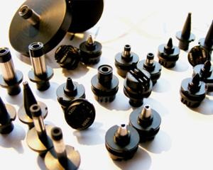
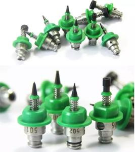
2. Pick and Place Machine: Automates the placement of components onto the PCB.
3. Reflow Oven: Heats the board to melt the solder paste and create strong electrical connections.
4. Soldering Iron: Useful for manual adjustments or rework.
5. Inspection Tools: Such as microscopes or cameras for checking solder joints.
Materials Required
- Printed Circuit Boards (PCBs): The base on which components are mounted.
- Solder Paste: A mixture of tiny solder balls and flux used to attach components to the PCB.
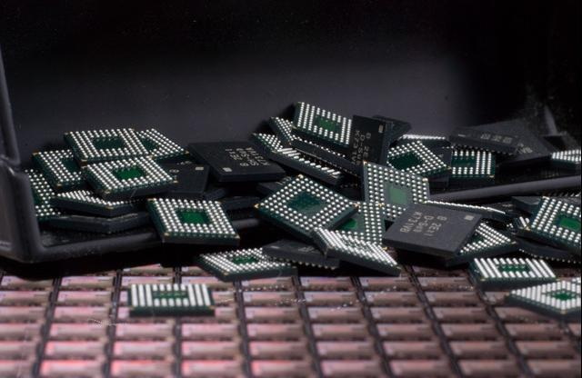
- Surface Mount Components: Resistors, capacitors, ICs, etc., designed for surface mounting.
The SMT PCB Assembly Process
Step 1: Design the PCB
The first step in SMT PCB assembly is designing the circuit board. This involves using software like Altium Designer or Eagle to create a schematic and layout. Key considerations include:
- Component placement
- Trace routing
- Pad sizes for different components
- Design rules for manufacturing
Step 2: Material Preparation
Before beginning the assembly process, all materials must be prepared and inspected for defects. This includes:
- Ensuring that PCBs are free from contaminants.
- Checking that surface mount devices (SMDs) are in good condition and correctly oriented.
Step 3: Print Solder Paste
Once the design is finalized, the next step is to print solder paste onto the PCB. This is done using a solder paste printer that aligns with the PCB's pads to ensure accurate application. Proper stencil thickness and alignment are crucial for achieving optimal results. The solder paste must be applied evenly; otherwise, it can lead to insufficient solder joints or solder bridging during reflow.
Step 4: Place Components
After applying solder paste, components are placed onto the PCB using a pick-and-place machine. This machine uses vision systems to accurately position each component on its designated pad. Manual placement may be necessary for prototypes or small runs but can introduce variability in placement accuracy.
Step 5: Reflow Soldering
Once all components are placed, the PCB is passed through a reflow oven. The oven heats the board in stages:
1. Preheat: Gradually raises the temperature to avoid thermal shock.
2. Soak: Maintains a steady temperature to activate flux in solder paste.
3. Reflow: Melts solder paste to form solid connections between components and pads.
4. Cooling: Rapidly cools down the board to solidify the solder joints.
Precise control of temperature profiles during this stage is critical; excessive heat can damage components while insufficient heat may result in poor solder joints.
Step 6: Cleaning
After reflowing, PCBs often require cleaning to remove any residual flux or contaminants that could affect performance. This can involve ultrasonic cleaning or using solvents designed specifically for electronics.
Step 7: Inspection
After cleaning, it's essential to inspect the board for defects such as cold solder joints or misaligned components. Automated Optical Inspection (AOI) systems can quickly identify issues by comparing images of the assembled board against a known good reference.
Step 8: Testing
Functional testing ensures that all components are working as intended. This may involve using specialized equipment to verify electrical characteristics or running firmware tests on assembled boards.

Common Challenges in SMT Assembly
Despite its advantages, SMT assembly can present several challenges:
Solder Bridging
Solder bridging occurs when excess solder connects two adjacent pads unintentionally, leading to short circuits. This often results from improper solder paste application or incorrect reflow profiles.
Insufficient Solder Joints
Insufficient solder joints can lead to electrical opens where connections fail due to inadequate solder coverage on component leads or pads. This issue may arise from clogged stencil apertures during printing or insufficient solder paste application.
Tombstoning
Tombstoning happens when one side of a component lifts off its pad during reflow while the other side remains attached. This defect is typically caused by uneven heating or imbalanced thermal profiles during reflow.
Non-Wetting or De-Wetting
Non-wetting occurs when solder fails to adhere properly to component leads or pads due to surface contamination or poor PCB finish quality. It can also result from inadequate flux activation during reflow.
Solder Balling
Solder balling refers to tiny spheres of solder forming near component leads due to moisture contamination in solder paste or improper reflow profiles. These can create unintended connections between adjacent pads.
Solutions to Common Challenges
To address these challenges effectively:
- Ensure proper training for operators handling equipment like stencil printers and pick-and-place machines.
- Implement strict quality control measures during each stage of production.
- Regularly calibrate equipment used in printing and reflow processes.
- Utilize automated inspection systems such as AOI or X-ray inspection for early detection of defects.
- Maintain optimal environmental conditions (temperature and humidity) during assembly processes to minimize issues related to moisture contamination.
Best Practices for SMT PCB Assembly
Design Considerations
- Ensure adequate spacing between components to allow for heat dissipation.
- Use appropriate pad sizes based on component specifications.
- Include test points in your design for easier testing later on.
Solder Paste Application
- Use a stencil that matches your pad layout precisely.
- Ensure that solder paste is applied evenly without excess or insufficient amounts.
Component Placement
- Utilize automated pick-and-place machines whenever possible for precision.
- For manual placement, use tweezers designed for handling small components.
Reflow Profile Optimization
- Optimize your reflow oven settings based on component types and solder paste specifications.
- Monitor temperatures closely during reflow to avoid overheating sensitive components.
Conclusion
SMT PCB assembly is an essential process in modern electronics manufacturing that offers numerous advantages over traditional methods. By understanding each step of the assembly process—from design through inspection—manufacturers can produce high-quality PCBs efficiently and cost-effectively. Adhering to best practices ensures optimal performance and reliability in electronic devices while mitigating common challenges associated with SMT assembly processes.

FAQ
1. What is the difference between SMT and through-hole technology?
SMT involves mounting components directly onto the surface of PCBs, while through-hole technology requires inserting leads into holes drilled in the board. SMT allows for higher density and smaller designs compared to through-hole technology.
2. What materials are required for SMT assembly?
Key materials include printed circuit boards (PCBs), solder paste, surface mount components (like resistors and capacitors), and sometimes additional materials like adhesives or conformal coatings depending on specific applications.
3. How does reflow soldering work?
Reflow soldering involves heating a PCB with applied solder paste in stages—preheating, soaking, reflowing (melting), and cooling—to create solid electrical connections between components and pads without damaging them.
4. What are common defects in SMT assembly?
Common defects include misaligned components, cold solder joints, insufficient solder application, bridging (where solder connects two pads), and component tombstoning (where one side of a component lifts off).
5. Can I perform SMT assembly at home?
While it's possible to perform SMT assembly at home using manual tools like a soldering iron and tweezers, achieving high-quality results typically requires specialized equipment like a reflow oven or pick-and-place machine for efficiency and precision.
Citations:
[1] https://jhdpcb.com/pcb-assembly/smt-assembly/
[2] https://levisonenterprises.com/5-advantages-to-using-smt/
[3] https://jhdpcb.com/blog/efficient-smt-assembly/
[4] https://www.ednasia.com/top-12-incredible-techniques-to-control-the-quality-of-pcb-smt-assembly/
[5] https://www.mpe-electronics.co.uk/2024/01/23/future-pcb-industry-trends-to-watch-out-for
[6] https://www.wevolver.com/article/smt-process
[7] https://www.pcbway.com/blog/PCB_Assembly/Advantages_and_Disadvantages_of_Surface_Mounting_Technology.html
[8] https://www.viasion.com/blog/common-challenges-in-smt-assembly-and-solutions/
[9] https://www.raypcb.com/surface-mount-technology/
[10] https://www.fs-pcba.com/smt-process-flow/


