Content Menu
● Use Proper Footprints
>> Importance of IPC Standards
>> Avoiding Common Footprint Mistakes
● Optimize Component Placement
>> Consideration of Thermal and Mechanical Factors
>> Placement for Testability and Repair
● Follow Design for Manufacturing (DFM) Guidelines
>> Communication with Your PCB Assembler
>> Common DFM Issues to Avoid
● Design for Solder Paste Printing
>> Stencil Design Considerations
>> Paste Volume and Component Size
● Include Test Points for Easy Troubleshooting
>> Types of Test Points
>> Test Point Placement Best Practices
● Consider PCB Material and Thickness
>> Common PCB Materials for SMT
>> Impact of Board Thickness on Assembly
● Optimize Via Design and Placement
>> Filled and Capped Vias
>> Via Stitching for Thermal Management
● Ensure Proper Thermal Management
>> Thermal Relief Pads vs. Solid Pads
>> Heat Sinks and Thermal Interface Materials
● Use Automated Optical Inspection (AOI) and X-ray Testing
>> Fiducial Markers
>> Accessibility for AOI
● Conclusion
● FAQ
>> 1. What is SMT PCB assembly?
>> 2. Why is footprint accuracy important in SMT PCB design?
>> 3. How does component placement affect SMT assembly?
>> 4. What role do DFM guidelines play in SMT PCB design?
>> 5. How can test points improve PCBA testing?
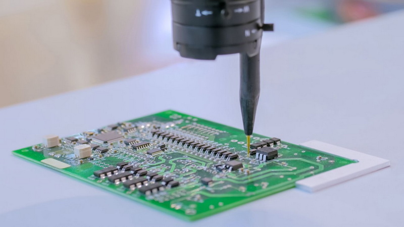
Optimizing PCB design for Surface Mount Technology (SMT) assembly is critical to achieving high-quality, reliable, and cost-effective printed circuit board assemblies (PCBA). SMT assembly involves placing electronic components directly onto the surface of a PCB, enabling faster production and higher component density compared to traditional through-hole assembly. However, the success of SMT assembly depends heavily on how well the PCB design is optimized to accommodate the assembly process.
This comprehensive guide covers essential strategies and best practices to optimize your PCB design for SMT assembly, focusing on key aspects such as footprint design, component placement, soldering considerations, and Design for Manufacturability (DFM) guidelines. By following these recommendations, you can improve assembly yield, reduce production costs, and enhance the overall performance of your PCBA.

Use Proper Footprints
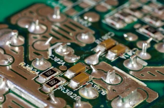
A fundamental step in optimizing your PCB design for SMT assembly is to use accurate and manufacturer-approved component footprints. Footprints define the size, shape, and pad layout of each surface mount device (SMD) on the PCB. Proper footprints ensure that components are correctly aligned during placement and soldering.
- Follow IPC standards for footprint design, including toe, heel, side, and periphery dimensions to facilitate proper solder fillets and avoid solder bridging.
- Use footprints recommended by component manufacturers or verified libraries from trusted sources.
- Ensure pad sizes and shapes match the soldering requirements to promote strong mechanical and electrical connections.
Proper footprints reduce placement errors and rework rates, improving the reliability of the final PCBA.
Importance of IPC Standards
The IPC (Institute for Printed Circuits) standards, such as IPC-7351, provide guidelines for creating footprints that optimize solder joint reliability and manufacturability. Adhering to these standards helps ensure compatibility with automated pick-and-place machines and solder paste printing processes.
Avoiding Common Footprint Mistakes
Common mistakes such as undersized pads, incorrect pad spacing, or missing solder mask dams can lead to solder bridging or tombstoning during SMT assembly. Double-checking footprints against datasheets and using footprint verification tools can prevent these issues.
Optimize Component Placement
Component placement significantly impacts the SMT assembly process flow and the electrical performance of the PCB. Good placement practices include:
- Group related components close together to minimize trace lengths, reduce signal degradation, and lower electromagnetic interference (EMI) and electromagnetic compatibility (EMC) issues.
- Arrange components logically to support the assembly sequence, facilitating efficient pick-and-place machine operation.
- Avoid placing components too close together to prevent solder bridging and allow for adequate solder paste application.
- Place passive components like resistors and capacitors near their corresponding IC pins to improve signal integrity.
- Keep polarized components oriented consistently to reduce assembly errors.
Optimized placement not only improves manufacturability but also enhances circuit performance and reduces production time.
Consideration of Thermal and Mechanical Factors
When placing components, consider heat dissipation requirements and mechanical stresses. For example, heat-generating components should be spaced to allow airflow or be placed near heat sinks. Mechanical stress points, such as connectors or heavy components, should be reinforced with additional pads or mounting holes.
Placement for Testability and Repair
Design your PCB layout to allow easy access for testing probes and rework tools. Avoid placing components in locations that obstruct test points or make manual soldering difficult.
Follow Design for Manufacturing (DFM) Guidelines
DFM guidelines are crucial for aligning your PCB design with the capabilities and constraints of the SMT assembly process. These guidelines are usually provided by your assembly house and include:
- Minimum spacing between components to avoid solder bridging.
- Orientation of components for optimal pick-and-place machine efficiency.
- Recommended pad sizes and shapes for solderability.
- Via sizes and locations that do not interfere with component pads.
- Placement of fiducials and tooling holes for accurate board alignment.
Adhering to DFM guidelines reduces assembly defects, minimizes manual intervention, and enhances production yield.
Communication with Your PCB Assembler
Early collaboration with your PCB assembler can help you understand their specific DFM requirements. This collaboration can prevent costly redesigns and delays by ensuring your design is fully compatible with their SMT assembly processes.
Common DFM Issues to Avoid
- Insufficient solder mask clearance around pads.
- Overlapping silkscreen on pads.
- Vias placed too close to pads causing solder wicking.
- Lack of fiducials for machine vision alignment.

Design for Solder Paste Printing
Solder paste printing is a critical SMT process step where solder paste is applied to the PCB pads through a stencil. To optimize this step:
- Ensure stencil apertures match the pad sizes and shapes accurately.
- Avoid overly large or small pads that can cause insufficient or excessive solder paste deposition.
- Design pads with rounded corners to improve solder paste release.
- Maintain consistent pad sizes for similar components to simplify stencil design.
Proper solder paste printing prevents solder joint defects such as tombstoning, bridging, and insufficient solder.
Stencil Design Considerations
The stencil thickness and aperture shape directly affect the volume of solder paste deposited. For fine-pitch components, laser-cut stencils with electro-polished apertures help achieve precise paste volumes and reduce defects.
Paste Volume and Component Size
Larger components require more solder paste, but excessive paste can cause bridging, while insufficient paste leads to weak joints. Balancing paste volume through optimized pad and stencil design is essential.
Include Test Points for Easy Troubleshooting
Incorporate test points in your PCB design to facilitate post-assembly testing and debugging. Test points allow measurement of signals at critical nodes without removing components.
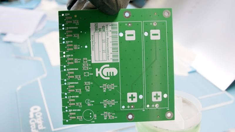
- Place test points in accessible locations away from dense component areas.
- Clearly mark test points on silkscreen layers for easy identification.
- Use standardized pad sizes for test points to accommodate probes.
Test points improve quality control and reduce troubleshooting time during PCBA testing.
Types of Test Points
Test points can be simple pads, vias, or dedicated test fixtures. Consider the test method (flying probe, bed-of-nails) when designing test points to ensure compatibility.
Test Point Placement Best Practices
Avoid placing test points under components or in areas where solder mask may cover them. Group test points logically to facilitate automated testing sequences.
Consider PCB Material and Thickness
The choice of PCB material and thickness affects SMT assembly quality and reliability:
- Use materials with suitable thermal properties to withstand reflow soldering temperatures.
- Select appropriate board thickness to balance mechanical strength and thermal dissipation.
- Consider copper thickness and layer stack-up to optimize signal integrity and heat management.
Material selection impacts solder joint quality and long-term PCBA performance.
Common PCB Materials for SMT
FR-4 is the most common PCB substrate due to its good mechanical and thermal properties. For high-frequency or high-power applications, materials like Rogers or polyimide may be preferred.
Impact of Board Thickness on Assembly
Thicker boards provide better mechanical support but may require longer reflow times. Thin boards are more flexible but can be prone to warping during soldering.
Optimize Via Design and Placement
Vias can influence soldering quality and electrical performance:
- Avoid placing vias directly under component pads unless they are filled and plated over to prevent solder wicking.
- Use via-in-pad technology carefully to maintain solder joint integrity.
- Maintain adequate spacing between vias and pads to avoid solder bridging.
Proper via design enhances manufacturability and circuit reliability.
Filled and Capped Vias
Filled and capped vias under pads prevent solder paste from flowing into the via barrel, which can cause insufficient solder joints. This technique is especially important for fine-pitch BGAs.
Via Stitching for Thermal Management
Via stitching around heat-generating components helps transfer heat to inner layers or heat sinks, improving thermal performance.
Ensure Proper Thermal Management
High-density SMT PCBs can generate significant heat, which affects component reliability:
- Use thermal relief pads and copper pours to dissipate heat efficiently.
- Place heat-sensitive components away from heat sources.
- Consider adding thermal vias to transfer heat to inner or opposite layers.
Thermal management prevents overheating and improves the lifespan of the PCBA.
Thermal Relief Pads vs. Solid Pads
Thermal relief pads connect component pads to copper pours through narrow traces, balancing heat dissipation and solderability. Solid pads can cause heat sinking issues during soldering.
Heat Sinks and Thermal Interface Materials
Incorporate heat sinks or thermal interface materials in the design for components that dissipate high power, ensuring efficient heat removal.
Use Automated Optical Inspection (AOI) and X-ray Testing
Design your PCB to accommodate inspection methods that detect assembly defects:
- Include fiducials for machine vision alignment.
- Design for accessibility of solder joints for AOI.
- For BGAs and hidden solder joints, plan for X-ray inspection.
These inspection techniques ensure defects are caught early, reducing costly rework.
Fiducial Markers
Fiducials are reference marks on the PCB that help pick-and-place machines align components accurately. Place at least three fiducials on each PCB panel.
Accessibility for AOI
Ensure that critical solder joints are visible to AOI cameras by avoiding overlapping silkscreen or components blocking the view.
Conclusion
Optimizing your PCB design for SMT assembly is a multi-faceted process that requires attention to detail in footprint design, component placement, soldering considerations, and manufacturability guidelines. By following best practices such as using proper footprints, adhering to DFM rules, designing for effective solder paste printing, and incorporating test points, you can significantly improve assembly yield, reduce production costs, and enhance the reliability of your PCBA.
Furthermore, considering material properties, thermal management, and inspection accessibility ensures your design is robust and ready for modern SMT assembly lines. Ultimately, a well-optimized SMT PCB design leads to faster production, fewer defects, and higher-quality electronic products.

FAQ
1. What is SMT PCB assembly?
SMT PCB assembly is the process of mounting surface mount components directly onto the surface of a printed circuit board (PCB) using automated machines and soldering techniques, enabling high-density and efficient electronic manufacturing.
2. Why is footprint accuracy important in SMT PCB design?
Accurate footprints ensure that components fit correctly on the PCB pads, allowing precise placement and reliable solder joints, which are essential for reducing assembly errors and improving product reliability.
3. How does component placement affect SMT assembly?
Proper component placement reduces trace lengths, minimizes electromagnetic interference, supports efficient pick-and-place operations, and prevents soldering defects, all of which contribute to a smoother assembly process and better electrical performance.
4. What role do DFM guidelines play in SMT PCB design?
DFM guidelines help designers align their PCB layouts with manufacturing capabilities and constraints, reducing defects, improving assembly efficiency, and lowering production costs.
5. How can test points improve PCBA testing?
Test points provide accessible locations for measuring electrical signals during testing and troubleshooting, facilitating quality control and faster identification of assembly issues.


