Content Menu
● Understanding SMT Stencil Technology
>> Importance of SMT Stencils in Soldering Quality
● Key Design Considerations for SMT Stencils
>> Aperture Size and Shape
>> Stencil Thickness
>> Aperture Design Innovations
● Materials and Manufacturing Methods
● Optimizing SMT Stencil Performance
>> Surface Treatments
>> Stencil Frame and Handling
>> Paste Volume and Printing Method
● Addressing Common Soldering Defects through Stencil Design
● Enhancing SMT Stencil Design with Advanced Software Tools
● Environmental Considerations in SMT Stencil Manufacturing
● Future Trends in SMT Stencil Technology
● Conclusion
● FAQ
>> 1. What is the role of SMT stencil technology in solder paste application?
>> 2. How does aperture size affect soldering quality?
>> 3. Why is stencil thickness important?
>> 4. What are some stencil design techniques to reduce soldering defects?
>> 5. What future developments are expected in SMT stencil technology?
Surface Mount Technology (SMT) stencil design plays a critical role in ensuring high-quality soldering in PCB assembly. SMT stencil technology enables precise and consistent application of solder paste onto PCB pads, which is essential for reliable solder joints and overall product performance. This article explores how to improve soldering quality through effective SMT stencil design, covering key design principles, materials, optimization techniques, and future trends.

Understanding SMT Stencil Technology
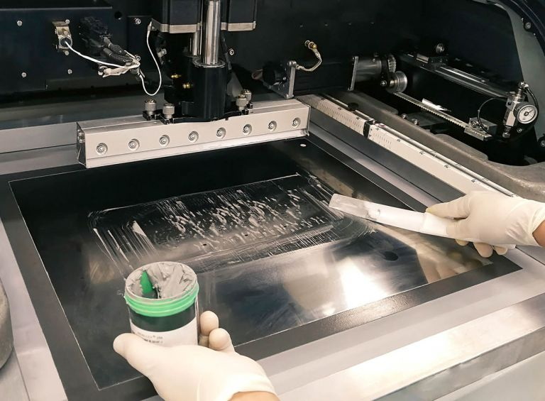
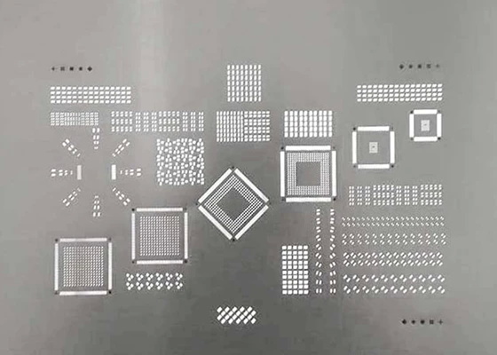
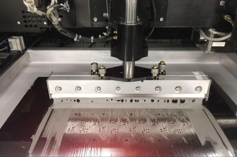
SMT stencils are thin metal sheets, usually made of stainless steel or nickel alloys, with laser-cut apertures that correspond exactly to the solder pad locations on a PCB. During the solder paste printing process, solder paste is applied through these apertures onto the PCB pads, enabling accurate deposition of the right amount of solder paste for each component.
Importance of SMT Stencils in Soldering Quality
- Accurate Paste Volume: Proper stencil design ensures the right volume of solder paste is deposited, preventing defects like insufficient solder or bridging.
- Consistent Paste Application: Stencils maintain uniformity across multiple boards, reducing variability and improving yield.
- Minimized Defects: Well-designed stencils reduce common soldering defects such as solder balls, tombstoning, and voiding.
Key Design Considerations for SMT Stencils
Aperture Size and Shape
The aperture size and shape directly influence the solder paste volume and joint quality. Common aperture shapes include rectangles, circles, and home plates. The aperture dimensions should slightly exceed the pad size to compensate for paste shrinkage during reflow, ensuring full coverage and strong solder joints.
- Aspect Ratio: The ratio of aperture width to stencil thickness should be at least 1.5 to ensure proper paste release.
- Area Ratio: The aperture surface area divided by the aperture wall area should be no less than 0.66 to maintain paste transfer efficiency.
Stencil Thickness
Stencil thickness affects the volume of solder paste deposited. Thinner stencils (around 0.005 inches) are preferred for fine-pitch components but may limit paste volume. Thicker stencils provide more paste but can cause paste release problems. Selecting the right thickness depends on component size, pitch, and solder paste characteristics.
Aperture Design Innovations
- Custom Apertures: Modified shapes like “U-Shape”, “Inverted Homeplate”, and “Reverse U-Shape” apertures can mitigate defects such as solder balls and tombstoning by controlling paste distribution more precisely.
- Step or Multi-level Apertures: These can be used to optimize paste volume for complex components or uneven pad layouts.
Materials and Manufacturing Methods
- Stainless Steel: The most common material for SMT stencils due to its durability and precision.
- Nickel Alloys: Used for specialized applications requiring enhanced wear resistance.
- Laser Cutting: The preferred method for aperture creation, offering high precision and repeatability, essential for fine-pitch components.
- Chemical Etching: A cost-effective alternative for larger apertures but less precise than laser cutting.

Optimizing SMT Stencil Performance
Surface Treatments
- Electropolishing: Smooths microscopic imperfections on stencil apertures, improving solder paste release and print quality.
- Nano-coating: Enhances stencil hydrophobicity, reducing paste sticking and cleaning frequency.
Stencil Frame and Handling
Framed stencils provide stability and consistent tension, crucial for high-volume production and automated printing processes. Proper handling and storage prevent damage that could degrade print quality.
Paste Volume and Printing Method
The stencil design must be compatible with the printing method (manual or automated) and solder paste properties (viscosity, particle size) to ensure consistent paste deposition.
Addressing Common Soldering Defects through Stencil Design
- Solder Balls: Use “U-Shape” or “Inverted Homeplate” apertures to reduce solder ball formation during reflow.
- Tombstoning: Adjust aperture size and shape, such as “Reverse U-Shape” apertures, to balance solder paste volume on both sides of two-pin components.
- Voiding: Optimize aperture coverage on ground pads (e.g., QFN devices) by following IPC 7525 guidelines, typically applying 20%-50% aperture coverage to reduce voids.
Enhancing SMT Stencil Design with Advanced Software Tools
Modern SMT stencil design benefits greatly from advanced software tools that allow engineers to simulate solder paste deposition and optimize aperture patterns before manufacturing. These tools help predict potential defects and improve stencil efficiency, reducing trial-and-error in production. Simulation software can model paste release behavior, thermal profiles during reflow, and component placement tolerances, enabling proactive adjustments to stencil design that improve soldering quality and yield.
Environmental Considerations in SMT Stencil Manufacturing
Sustainability is becoming increasingly important in electronics manufacturing. Choosing environmentally friendly materials and processes for stencil production, such as recyclable stainless steel and low-impact laser cutting, contributes to greener manufacturing practices. Additionally, optimizing stencil life through durable coatings and proper maintenance reduces waste and resource consumption, aligning SMT stencil technology with global sustainability goals.
Future Trends in SMT Stencil Technology
- 3D-Printed Stencils: Additive manufacturing enables complex, multi-level stencil designs that can handle diverse component sizes on a single PCB.
- Smart Stencils: Integration of sensors and real-time data collection to monitor print quality and stencil wear, enabling proactive maintenance and process optimization.
- Adaptive Stencil Designs: Future stencils may incorporate dynamic aperture adjustments or modular components to quickly adapt to different PCB layouts, reducing downtime and tooling costs.
Conclusion
Improving soldering quality with SMT stencil design requires a holistic approach that balances aperture size and shape, stencil thickness, material choice, and manufacturing precision. Leveraging innovative aperture designs and surface treatments can significantly reduce soldering defects such as solder balls, tombstoning, and voiding. Advanced software tools and sustainable manufacturing practices further enhance stencil performance and environmental responsibility. As SMT stencil technology evolves with 3D printing and smart features, manufacturers will achieve higher yields, better reliability, and streamlined production processes.

FAQ
1. What is the role of SMT stencil technology in solder paste application?
SMT stencil technology ensures precise and consistent deposition of solder paste onto PCB pads, which is critical for forming reliable solder joints and minimizing defects during SMT assembly.
2. How does aperture size affect soldering quality?
Aperture size determines the volume of solder paste deposited. If too small, it leads to insufficient solder; if too large, it can cause bridging or solder balls. Proper sizing slightly larger than the pad size is recommended to compensate for paste shrinkage.
3. Why is stencil thickness important?
Stencil thickness controls the amount of solder paste deposited. Thinner stencils suit fine-pitch components but may limit paste volume, while thicker stencils provide more paste but risk poor paste release. Balancing thickness is key to optimal soldering.
4. What are some stencil design techniques to reduce soldering defects?
Techniques include using specialized aperture shapes like “U-Shape” or “Inverted Homeplate” to reduce solder balls and “Reverse U-Shape” to mitigate tombstoning. Optimizing aperture coverage on ground pads helps reduce voiding.
5. What future developments are expected in SMT stencil technology?
Future trends include 3D-printed multi-level stencils for complex PCB layouts and smart stencils with embedded sensors for real-time print quality monitoring and maintenance.


