Content Menu
● Understanding SMT PCB Shielding
>> What is SMT PCB Shield?
>> Importance of SMT PCB Shielding
● Key Materials for SMT PCB Shielding
● SMT Shield Types and Mounting Methods
>> Surface Mount Device (SMD) Shields vs. SMT Shields
>> SnapShot Surface Mount Shields
● Design Considerations for Effective SMT PCB Shielding
>> 1. Identify EMI Sources and Sensitive Components
>> 2. Layer Stack-Up and Ground Planes
>> 3. Shield Coverage and Placement
>> 4. Use of Copper Shields
>> 5. Consider Frequency Range
>> 6. Thermal Management
>> 7. Manufacturing and Cost
● Practical Steps to Design SMT PCB Shielding
>> Step 1: PCB Layout Optimization
>> Step 2: Define Shielding Zones
>> Step 3: Select Shielding Method
>> Step 4: Design Shield Attachments
>> Step 5: Verify Shield Effectiveness
● Advanced Shielding Techniques
>> Copper Shield Layers
>> Conductive Coatings
>> Shielding Films
● Avoiding SMT Component Issues During Shielding
● Conclusion
● FAQ
>> 1. What is the difference between SMT and SMD shields?
>> 2. How does copper shielding work in SMT PCB shields?
>> 3. Can SMT shields be removed for repair?
>> 4. What design considerations help avoid SMT component tombstoning?
>> 5. How do I choose the right shielding material for my PCB?
● Citations:
In modern electronics, electromagnetic interference (EMI) and radio frequency interference (RFI) pose significant challenges to device performance and reliability. Surface Mount Technology (SMT) PCB shields have become essential components in mitigating these issues by protecting sensitive circuits from external and internal noise sources. This comprehensive guide explores the principles, materials, design strategies, and practical considerations for designing a PCB with effective SMT shielding, focusing on the keyword smt pcb shield throughout.

Understanding SMT PCB Shielding
What is SMT PCB Shield?
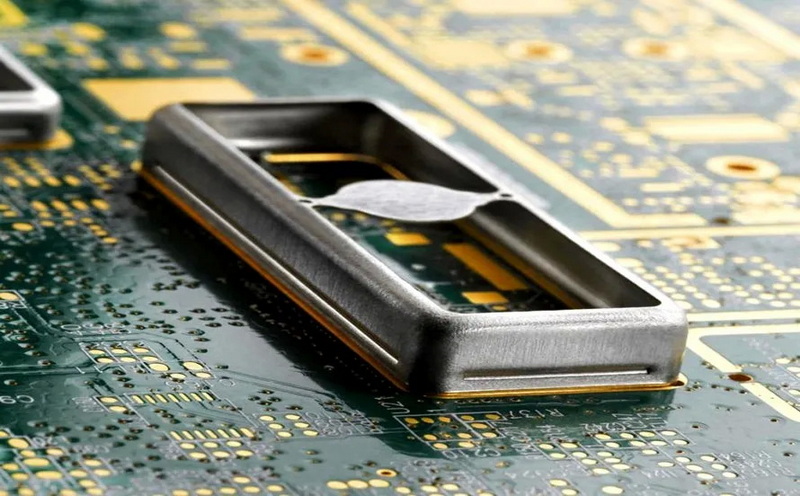
SMT PCB shield refers to electromagnetic shielding solutions that are mounted directly onto the surface of a printed circuit board (PCB) using surface mount technology. These shields can be metallic covers or coatings that protect sensitive components from EMI and RFI, ensuring signal integrity and device reliability.
Importance of SMT PCB Shielding
- Noise Reduction: Prevents electromagnetic noise from affecting sensitive components.
- Signal Integrity: Maintains the quality of high-frequency signals.
- Compliance: Helps meet regulatory standards for EMI emissions.
- Device Reliability: Reduces malfunction and data errors caused by interference.
Key Materials for SMT PCB Shielding
Choosing the right material is crucial for effective shielding. The most common materials include:
| Material | Properties | Advantages | Disadvantages |
| Copper | High electrical conductivity | Excellent EMI shielding, flexible design | Prone to oxidation, requires plating |
| Nickel Silver | Good conductivity and corrosion resistance | Durable, strong, solderable | Higher cost |
| Tin-Plated Steel | Strong and cost-effective | Corrosion protection, good solderability | Lower conductivity than copper |
Copper is the most widely used due to its superior conductivity, but it often requires tin plating to prevent oxidation and improve solderability[9].
SMT Shield Types and Mounting Methods
Surface Mount Device (SMD) Shields vs. SMT Shields
- SMD Shield: A specific type of shield that is itself a surface mount device soldered onto the PCB.
- SMT Shield: A broader term encompassing any shield mounted using surface mount technology, including SMD shields and larger multi-component covers[6].
SnapShot Surface Mount Shields
A notable modern solution is the SnapShot surface mount shield system, where shields are snapped onto small solder spheres on the PCB surface. This allows easy removal and replacement without additional heating, facilitating quick repair and inspection[6][8].
Design Considerations for Effective SMT PCB Shielding
1. Identify EMI Sources and Sensitive Components
Pinpoint areas on the PCB that are susceptible to EMI or generate interference. Shielding should be placed as close as possible to these sources for maximum effectiveness[4].
2. Layer Stack-Up and Ground Planes
Incorporate dedicated ground planes and copper pours to create effective barriers against EMI. The PCB stack-up should be designed to integrate shielding layers that form enclosed cavities around sensitive circuits[1][4].
3. Shield Coverage and Placement
Ensure that the shield covers the entire area of the sensitive components or circuits. Shields should ideally extend to the part outline to simplify manufacturing and improve alignment[3].
4. Use of Copper Shields
Copper shields are simple to implement by adding external copper layers or pours. Additional vias may be necessary to maintain connectivity to SMT components beneath the shield[3][5].
5. Consider Frequency Range
Select shielding materials and thickness based on the frequency range of the interference. Different materials perform better at different frequencies[4].
6. Thermal Management
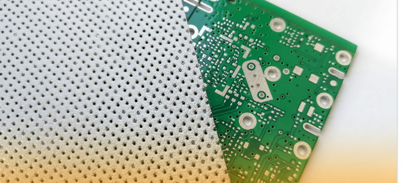
Design shields with holes or slots if heat dissipation is a concern. Some SMT shields can be customized to include ventilation features without compromising shielding effectiveness[6].
7. Manufacturing and Cost
Balance the shielding effectiveness with manufacturing complexity and cost. Some advanced shielding methods, such as silver ink or shielding films, may increase production costs[3].

Practical Steps to Design SMT PCB Shielding
Step 1: PCB Layout Optimization
- Maintain proper trace spacing to reduce crosstalk.
- Use continuous ground planes to minimize EMI.
- Place sensitive components away from noisy circuits[2].
Step 2: Define Shielding Zones
- Create shielded zones on the PCB layout for critical components.
- Use copper pours or dedicated shield layers in these zones[3].
Step 3: Select Shielding Method
- Choose between copper shields, conductive coatings, or physical shield cans based on application needs.
- For removable shields, consider SnapShot technology for easy maintenance[5][6][8].
Step 4: Design Shield Attachments
- For SMT shields, design solder pads or spheres to attach the shield securely.
- Ensure electrical continuity between the shield and ground plane[6].
Step 5: Verify Shield Effectiveness
- Simulate EMI shielding performance using PCB design software.
- Conduct physical testing to validate shielding in real-world conditions[1][8].
Advanced Shielding Techniques
Copper Shield Layers
Adding external copper pour layers as shields is a straightforward and effective EMI mitigation technique. This method is universally supported by CAD tools and can be combined with vias for connectivity[3].
Conductive Coatings
Applying conductive epoxies or paints on PCB surfaces can create a conductive shield layer. This approach is flexible but may add complexity to manufacturing[5].
Shielding Films
Shielding films act as a secondary coverlay, providing a balance between copper shields and conductive inks. They require precise manufacturing tolerances and are useful in rigid-flex PCB designs[3].
Avoiding SMT Component Issues During Shielding
A common problem in SMT PCB design is the "tombstoning" or "standing up" of components during soldering due to uneven solder paste melting. Recent design methods involve creating pad restriction zones around SMT pads to control solder flow and improve component stability during reflow soldering[7].
Conclusion
Designing a PCB with effective SMT shielding requires a thorough understanding of EMI sources, shielding materials, and mounting techniques. Copper remains the preferred material for its conductivity and shielding performance, but considerations such as oxidation and cost must be addressed. Modern SMT shields, including removable SnapShot types, offer flexible and efficient EMI protection. By carefully planning shield placement, PCB stack-up, and manufacturing methods, engineers can significantly enhance device reliability and compliance with EMI standards.

FAQ
1. What is the difference between SMT and SMD shields?
Answer: SMD shields are specific surface mount devices soldered onto the PCB, while SMT shields refer more broadly to any shield mounted using surface mount technology, including SMD shields and larger covers[6].
2. How does copper shielding work in SMT PCB shields?
Answer: Copper shields act as conductive barriers that reflect and absorb electromagnetic waves, reducing EMI. They can be implemented as copper pours or layers on the PCB and require vias for connectivity to SMT components[3][5].
3. Can SMT shields be removed for repair?
Answer: Yes, technologies like SnapShot surface mount shields allow shields to be snapped on and off without additional heating, facilitating easy repair and inspection[6][8].
4. What design considerations help avoid SMT component tombstoning?
Answer: Creating pad restriction zones around SMT pads controls solder paste flow, preventing uneven melting that causes components to stand up during reflow soldering[7].
5. How do I choose the right shielding material for my PCB?
Answer: Consider factors such as electrical conductivity, corrosion resistance, mechanical strength, frequency range of EMI, and cost. Copper is common for high conductivity, nickel silver for durability, and tin-plated steel for cost-effective shielding[9].
Citations:
[1] https://resources.altium.com/p/emi-shielding-techniques
[2] https://www.nextpcb.com/blog/printed-circuit-board-shielding
[3] https://blog.epectec.com/demystifying-shielding-methods-in-gerber-designs
[4] https://www.elepcb.com/blog/pcb-shielding-basics-to-emi-and-rfi/
[5] https://xgrtec.com/blog/know-some-popular-emi-shielding-techniques/
[6] https://xgrtec.com/emi-rfi-shields/surface-mount-shields/
[7] https://patents.google.com/patent/WO2019024351A1/zh
[8] https://xgrtec.com/blog/removable-shielding-technologies-for-pcbs/
[9] https://www.precisionmicro.com/pcb-shielding-explained/


