Content Menu
● Understanding SMT and Populated PCBs
>> What is Surface-Mount Technology (SMT)?
>> The Difference Between Populated and Bare PCBs
● The SMT Assembly Process
>> 1. Solder Paste Application
>> 2. Component Placement
>> 3. Reflow Soldering
>> 4. Inspection
>> 5. Cleaning
>> 6. Testing
● Advantages of SMT
>> Additional Benefits
● Challenges Associated with SMT
>> Additional Challenges
● Factors Influencing SMT Assembly
>> Environmental Considerations
● Future Trends in SMT
● Conclusion
● FAQ
>> 1. What is a populated PCB?
>> 2. How does surface-mount technology differ from through-hole technology?
>> 3. What are some common applications for SMT?
>> 4. What challenges does SMT face in manufacturing?
>> 5. Why is inspection important in the SMT process?
● Citations:
Populating printed circuit boards (PCBs) with surface-mount technology (SMT) components is a crucial process in modern electronics manufacturing. This method allows for the efficient assembly of complex electronic devices, enabling manufacturers to produce smaller, lighter, and more powerful products. In this article, we will explore the various aspects of SMT, including its processes, advantages, challenges, and its impact on the electronics industry.

Understanding SMT and Populated PCBs
What is Surface-Mount Technology (SMT)?
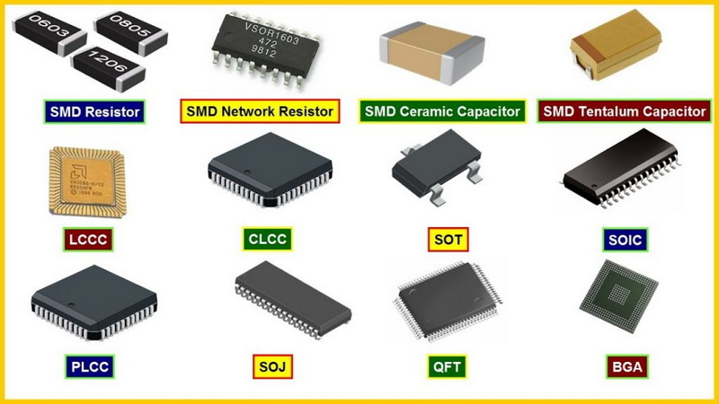
Surface-mount technology is a method of mounting electronic components directly onto the surface of a PCB. Unlike traditional through-hole technology, where components are inserted into holes drilled in the board, SMT components are soldered onto pads on the board's surface. This technique has revolutionized PCB assembly by allowing for higher component density and more compact designs.
The Difference Between Populated and Bare PCBs
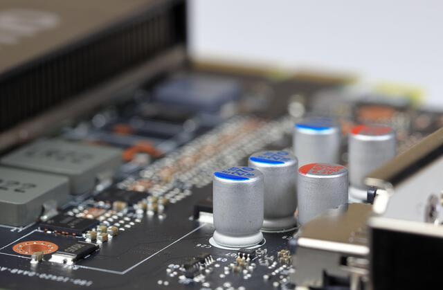
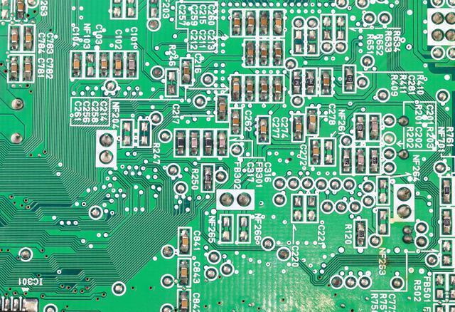
A populated PCB is one that has electronic components soldered onto it, while a bare PCB is simply a blank board without any components. The process of populating a PCB involves several critical steps that ensure the components are securely attached and function correctly.
The SMT Assembly Process
The SMT assembly process consists of several key steps:
1. Solder Paste Application
The first step in the SMT assembly process is applying solder paste to the PCB. Solder paste is a mixture of solder alloy and flux that helps create electrical connections between the components and the board. A stencil is often used to apply the paste accurately to the pads designated for component placement. The application of solder paste must be precise; too much paste can lead to bridging between pads, while too little can result in weak joints.
2. Component Placement
Once the solder paste has been applied, the next step involves placing the surface-mount devices (SMDs) onto the board. This is typically done using automated pick-and-place machines that can position components with high precision. These machines use vision systems to identify component placement and ensure accuracy. The speed and efficiency of these machines allow manufacturers to achieve high throughput in production.
3. Reflow Soldering
After component placement, the PCB is passed through a reflow oven where heat melts the solder paste, creating strong electrical connections between the components and the pads on the PCB. This step is critical as it solidifies the connections necessary for proper functionality. The reflow process involves several temperature zones: preheating, soaking, reflow, and cooling. Each zone plays a vital role in ensuring that all components are properly soldered without damaging sensitive parts.
4. Inspection
Post-soldering inspection is essential to ensure that all components are correctly placed and soldered. Automated optical inspection (AOI) systems are commonly used to detect any defects or misalignments. These systems can quickly scan PCBs for issues such as missing components, misaligned parts, or insufficient solder joints. Manual inspection may also be performed for critical applications where reliability is paramount.
5. Cleaning
After inspection, any residual flux or contaminants are cleaned from the PCB to ensure optimal performance and longevity of the assembled device. Cleaning methods can include ultrasonic cleaning or using solvent-based cleaners to remove flux residues that could affect electrical performance over time.
6. Testing
Finally, functional testing is performed to verify that the populated PCB operates according to its specifications before it moves on to packaging and distribution. Testing can involve various methods such as in-circuit testing (ICT), functional testing, or boundary scan testing depending on the complexity of the circuit.
Advantages of SMT
SMT offers several advantages over traditional through-hole technology:
- Higher Component Density: SMT allows for more components to be placed in a smaller area, which is essential for modern compact electronic devices.
- Improved Performance: The shorter leads used in SMT reduce inductance and capacitance, which can enhance signal integrity.
- Automated Assembly: The use of automated machines for placement and soldering increases production speed and reduces labor costs.
- Flexibility: Components can be mounted on both sides of a PCB, allowing for more complex designs.
- Reduced Weight: The smaller size of SMT components contributes to lighter overall product designs.

Additional Benefits
Beyond these primary advantages, SMT also supports advanced technologies such as:
- Multi-layer Boards: SMT facilitates multi-layer PCB designs where multiple layers can be densely populated with components.
- Integration with Other Technologies: SMT allows for easy integration with other technologies like embedded passive components or chip-on-board configurations.
- Cost Efficiency: While initial setup costs for SMT equipment may be higher than traditional methods, mass production often leads to lower per-unit costs due to reduced material waste and faster assembly times.
Challenges Associated with SMT
Despite its advantages, SMT also presents certain challenges:
- Thermal Management: Smaller components can generate significant heat, requiring careful thermal management strategies in design.
- Component Handling: The tiny size of SMDs makes them more challenging to handle during assembly and increases the risk of damage.
- Repairability: SMT boards can be more difficult to repair than through-hole boards due to their compact nature and lack of access points for component replacement.
Additional Challenges
Moreover, there are other challenges that manufacturers face:
- Design Complexity: Designing PCBs for SMT requires specialized software tools and knowledge about component specifications to avoid issues during assembly.
- Supply Chain Issues: Sourcing high-quality SMDs can sometimes be problematic due to fluctuating market demands or shortages in specific components.
Factors Influencing SMT Assembly
Several factors can influence the effectiveness of SMT assembly:
- Component Size: The size and shape of components can affect placement speed and accuracy.
- Board Design: Complex designs may require additional consideration during assembly to avoid errors.
- Production Volume: High-volume production may necessitate different approaches compared to low-volume or prototype runs.
Environmental Considerations
As environmental concerns grow within manufacturing sectors, companies are increasingly focusing on sustainable practices:
- Lead-Free Soldering: Many manufacturers have transitioned to lead-free soldering processes due to regulations like RoHS (Restriction of Hazardous Substances), which aim to reduce hazardous materials in electronics.
- Energy Efficiency: Implementing energy-efficient practices within reflow ovens and other machinery not only reduces costs but also minimizes environmental impact.
Future Trends in SMT
The future of SMT looks promising as technology continues to evolve:
- Miniaturization: As devices become smaller and more powerful, there will be an increased demand for even smaller SMDs that maintain high performance.
- Advanced Materials: New materials such as flexible substrates will enable innovative designs for wearables and other applications requiring flexibility.
- Automation: Continued advancements in robotics will further streamline assembly processes, improving efficiency while reducing human error.
Conclusion
The process of populating PCBs with SMT components has become a cornerstone of modern electronics manufacturing. By enabling higher component densities, improving performance, and allowing for automated assembly processes, SMT has transformed how electronic devices are designed and produced. As technology continues to evolve, so too will the methods used for PCB population, ensuring that manufacturers can meet consumer demands for smaller, more efficient products while addressing challenges related to sustainability and repairability.

FAQ
1. What is a populated PCB?
A populated PCB is a printed circuit board that has electronic components soldered onto it, making it ready for use in electronic devices.
2. How does surface-mount technology differ from through-hole technology?
Surface-mount technology involves mounting components directly on the surface of a PCB without drilling holes, while through-hole technology requires inserting component leads into holes drilled into the board.
3. What are some common applications for SMT?
SMT is widely used in consumer electronics, telecommunications equipment, automotive systems, medical devices, and many other applications where compactness and efficiency are critical.
4. What challenges does SMT face in manufacturing?
Challenges include thermal management issues due to smaller component sizes, difficulties in handling tiny SMDs during assembly, and complications related to repairing SMT boards compared to traditional through-hole boards.
5. Why is inspection important in the SMT process?
Inspection ensures that all components are correctly placed and soldered before final testing and packaging, reducing defects and ensuring product reliability.
Citations:
[1] https://www.raypcb.com/populated-circuit-board/
[2] https://www.hemeixinpcb.com/company/news/what-is-the-smt-assembly-process.html
[3] https://www.wevolver.com/article/smt-process
[4] https://www.elepcb.com/blog/what-is-populated-pcb/
[5] https://www.protoexpress.com/kb/smt-assembly/
[6] https://jlcpcb.com/blog/the-characteristics-of-surface-mount-technology
[7] https://www.pcbbuy.com/news/What-is-Populated-PCB-&-What-is-the-Process-of-It.html
[8] https://jhdpcb.com/pcb-assembly/smt-assembly/
[9] https://www.protoexpress.com/blog/good-not-so-good-sides-surface-mount-technology/
[10] https://www.raypcb.com/populated-pcb/
[11] https://www.viasion.com/blog/what-are-the-steps-in-smt-assembly-process/


