Content Menu
● Understanding SMT Assembly
● The SMT Assembly Process: A Step-by-Step Guide
>> 1. PCB Design and Preparation
>> 2. Component Preparation
>> 3. Solder Paste Application
>> 4. Component Placement
>> 5. Reflow Soldering
>> 6. Inspection and Quality Control
>> 7. Additional Processes (if required)
>> 8. Final Testing and Packaging
● The Importance of SMT in Modern Electronics
● Challenges in SMT Assembly
● Future Trends in SMT Assembly
● Conclusion
● FAQ
>> 1. What are the main advantages of SMT over through-hole technology?
>> 2. How does the reflow soldering process work in SMT assembly?
>> 3. What are some common defects in SMT assembly and how are they detected?
>> 4. How has SMT assembly evolved in recent years?
>> 5. What are the key considerations when designing a PCB for SMT assembly?
● Citations:
Surface Mount Technology (SMT) has revolutionized the electronics manufacturing industry, enabling the production of smaller, more complex, and more efficient printed circuit boards (PCBs). This article will delve into the intricacies of the SMT assembly process, exploring each step from start to finish, and highlighting the crucial role it plays in modern electronics manufacturing.

Understanding SMT Assembly
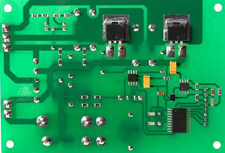
SMT assembly is a method of producing electronic circuits where components are mounted directly onto the surface of printed circuit boards. This technique has largely replaced the older through-hole technology, offering numerous advantages in terms of miniaturization, performance, and production efficiency.
The SMT Assembly Process: A Step-by-Step Guide
1. PCB Design and Preparation
The SMT assembly process begins long before any components are placed on the board. It starts with the careful design of the PCB itself. Engineers must consider factors such as component placement, trace routing, and thermal management to ensure optimal performance and manufacturability.
Once the design is finalized, the PCB is manufactured. The bare board typically features flat, metallic pads (usually copper plated with tin-lead, silver, or gold) known as solder pads. These pads serve as the mounting points for the surface mount components[1].
2. Component Preparation
While the PCBs are being prepared, the components that will be mounted on them are also readied for assembly. This involves:
- Bill of Materials (BOM) Creation: A comprehensive list of all components required for the assembly is generated.
- Component Kitting: The necessary parts are retrieved from stock and organized into assembly kits.
- Component Inspection: Each component is carefully examined for any defects or damage[5].
3. Solder Paste Application
The next crucial step in the SMT assembly process is the application of solder paste to the PCB. Solder paste, a sticky mixture of tiny solder particles and flux, is applied to the solder pads on the PCB. This is typically done using a stencil printing process:
- A metal stencil, precisely matched to the PCB design, is placed over the board.
- Solder paste is spread across the stencil using a squeegee, typically at an angle between 45° and 60°.
- When the stencil is removed, small deposits of solder paste remain on the solder pads[7].
The accuracy of this step is critical, as it directly affects the quality of the final solder joints.
4. Component Placement
Once the solder paste has been applied, the PCB moves to the component placement phase. This is where surface mount components (SMCs) are positioned onto the board. Modern SMT assembly lines use sophisticated pick-and-place machines for this task:
- Components are loaded into the machine in reels, trays, or tubes.
- The machine uses vacuum nozzles or mechanical grippers to pick up each component.
- Using programmed coordinates, the machine precisely places each component onto its designated position on the PCB.
These machines are incredibly fast and accurate, with some advanced models capable of placing up to 80,000 components per hour[9].

5. Reflow Soldering
After all components have been placed, the PCB undergoes reflow soldering. This process melts the solder paste, creating permanent electrical and mechanical connections between the components and the PCB. The reflow process typically involves several stages:
1. Preheat Zone: The PCB enters a preheat zone where its temperature is gradually raised to about 150°C. This helps to activate the flux in the solder paste and prepare the board for soldering.
2. Soak Zone: The board is held at a temperature between 150°C and 190°C for 60-120 seconds. This allows for thermal equalization across the PCB and components.
3. Reflow Zone: The temperature is rapidly increased to the peak temperature (usually between 210°C and 250°C). This causes the solder to melt and form joints between the components and the PCB.
4. Cooling Zone: The PCB is gradually cooled to solidify the solder joints[7].
The entire reflow process is carefully controlled to ensure optimal solder joint formation without damaging heat-sensitive components.
6. Inspection and Quality Control
After reflow soldering, the assembled PCBs undergo rigorous inspection and testing:
- Visual Inspection: Trained operators or automated optical inspection (AOI) systems check for visible defects such as misaligned components or solder bridges.
- X-ray Inspection: For components with hidden solder joints (like BGAs), X-ray inspection may be used to check for proper soldering.
- Electrical Testing: The PCBs are tested to ensure all electrical connections are correct and functioning as intended.
Any defects found during this stage are either reworked or, if irreparable, the board is scrapped[7].
7. Additional Processes (if required)
Depending on the complexity of the PCB and the specific requirements of the product, additional steps may be necessary:
- Double-sided Assembly: If components need to be mounted on both sides of the PCB, the process of paste application, component placement, and reflow soldering is repeated for the second side.
- Through-hole Component Insertion: Some designs may still require certain through-hole components. These are typically added after SMT assembly and soldered using wave soldering or selective soldering techniques.
- Conformal Coating: For PCBs that will be exposed to harsh environments, a protective conformal coating may be applied.
8. Final Testing and Packaging
Once all assembly steps are complete, the PCBs undergo final functional testing to ensure they meet all performance specifications. Passing boards are then cleaned, if necessary, and packaged for shipping or further integration into larger systems.
The Importance of SMT in Modern Electronics
The SMT assembly process has become the backbone of modern electronics manufacturing for several reasons:
1. Miniaturization: SMT allows for much higher component density on PCBs, enabling the creation of smaller, lighter electronic devices.
2. Improved Performance: The shorter connections between components in SMT assemblies can lead to better electrical performance, especially in high-frequency applications.
3. Cost-Effectiveness: While the initial setup costs for SMT can be high, the process is highly automated and efficient, reducing labor costs and increasing throughput.
4. Reliability: Properly executed SMT assembly can result in very reliable solder joints and overall product durability.
5. Flexibility: SMT is adaptable to a wide range of product types and volumes, from prototypes to high-volume production runs.
Challenges in SMT Assembly
Despite its many advantages, SMT assembly does present some challenges:
- Component Size: As components continue to shrink, placement accuracy becomes increasingly critical.
- Thermal Management: The dense packing of components can lead to heat dissipation issues.
- Solder Joint Reliability: Factors like thermal cycling and mechanical stress can affect the long-term reliability of solder joints.
- Inspection Difficulties: Some defects, particularly those under BGA components, can be difficult to detect without specialized equipment.
Future Trends in SMT Assembly
The field of SMT assembly continues to evolve, driven by the ever-increasing demands of the electronics industry. Some emerging trends include:
- 3D Printing in Electronics: Additive manufacturing techniques are being explored for creating PCBs and even some electronic components.
- Artificial Intelligence in Assembly: AI and machine learning are being integrated into SMT processes for improved efficiency and defect detection.
- Green Manufacturing: There's a growing focus on environmentally friendly materials and processes in SMT assembly.
- Industry 4.0 Integration: SMT assembly lines are becoming more connected and data-driven, aligning with Industry 4.0 principles.
Conclusion
The SMT assembly process is a marvel of modern manufacturing, combining precision engineering, advanced materials science, and high-speed automation. From the initial PCB design to the final quality control checks, each step in the process plays a crucial role in producing the reliable, compact electronic devices we rely on every day.
As technology continues to advance, SMT assembly will undoubtedly evolve to meet new challenges. However, its fundamental principles - the precise placement of components onto PCB surfaces and the use of reflow soldering to create reliable connections - will likely remain at the heart of electronics manufacturing for years to come.
Understanding the intricacies of the SMT assembly process is crucial for anyone involved in electronics design or manufacturing. By appreciating the capabilities and limitations of this technology, engineers and manufacturers can push the boundaries of what's possible in electronic devices, continuing to drive innovation in our increasingly connected world.

FAQ
1. What are the main advantages of SMT over through-hole technology?
SMT offers several advantages over through-hole technology:
- Miniaturization: SMT allows for much higher component density, resulting in smaller and lighter PCBs.
- Improved Performance: Shorter connections between components can lead to better electrical performance, especially at high frequencies.
- Automated Assembly: SMT is highly compatible with automated assembly processes, increasing production efficiency.
- Cost-Effectiveness: While initial setup costs can be high, SMT generally results in lower production costs for medium to high-volume manufacturing.
- Double-Sided Assembly: SMT makes it easier to place components on both sides of a PCB, further increasing circuit density.
2. How does the reflow soldering process work in SMT assembly?
Reflow soldering in SMT assembly typically involves four main stages:
1. Preheat: The PCB is gradually heated to activate the flux in the solder paste and prepare components for soldering.
2. Thermal Soak: The board is held at a steady temperature to ensure even heating across all components.
3. Reflow: The temperature is raised above the melting point of the solder, causing it to liquefy and form joints.
4. Cooling: The board is gradually cooled to solidify the solder joints.
This process is carefully controlled to ensure proper solder joint formation without damaging heat-sensitive components.
3. What are some common defects in SMT assembly and how are they detected?
Common defects in SMT assembly include:
- Solder Bridges: Excess solder connecting adjacent pads or leads.
- Tombstoning: One end of a component lifts off the board during reflow.
- Insufficient Solder: Not enough solder to form a proper joint.
- Component Misalignment: Components not correctly positioned on their pads.
These defects are typically detected through a combination of methods:
- Visual Inspection (manual or automated)
- X-ray Inspection (especially for hidden joints under BGAs)
- Automated Optical Inspection (AOI)
- In-Circuit Testing (ICT)
- Functional Testing
4. How has SMT assembly evolved in recent years?
SMT assembly has seen several advancements in recent years:
- Increased Miniaturization: Components and solder joints continue to shrink, allowing for even denser PCBs.
- Improved Automation: Pick-and-place machines have become faster and more accurate.
- Advanced Inspection Techniques: 3D AOI and advanced X-ray systems have improved defect detection.
- Lead-Free Soldering: Environmental regulations have driven the adoption of lead-free solder pastes.
- Industry 4.0 Integration: SMT lines are becoming more connected, with real-time data collection and analysis.
5. What are the key considerations when designing a PCB for SMT assembly?
When designing a PCB for SMT assembly, key considerations include:
- Component Selection: Choose components suitable for SMT assembly.
- Pad Design: Ensure proper pad sizes and shapes for each component type.
- Component Spacing: Allow adequate space between components for pick-and-place machines and to avoid solder bridging.
- Thermal Management: Consider heat dissipation, especially for high-power components.
- Test Point Access: Design in test points for in-circuit testing.
- Fiducial Marks: Include fiducial marks for machine vision alignment.
- DFM (Design for Manufacturability): Follow best practices to ensure the design is optimized for SMT assembly processes.
Citations:
[1] https://www.pcbonline.com/blog/smt-manufacturing-process.html
[2] https://patents.google.com/patent/CN112040669B/zh
[3] https://www.viasion.com/blog/what-are-the-steps-in-smt-assembly-process/
[4] https://www.wevolver.com/article/smt-process
[5] https://www.protoexpress.com/kb/smt-assembly/
[6] https://baike.baidu.com/item/%E7%94%B5%E5%AD%90%E7%BB%84%E8%A3%85%E6%8A%80%E6%9C%AF%E4%B8%93%E4%B8%9A%E8%8B%B1%E8%AF%AD/12086345
[7] https://insightsolutionsglobal.com/smt-surface-mount-technology-manufacturing-process/
[8] https://blogs.sw.siemens.com/valor-dfm-solutions/how-to-optimize-pcb-design-for-the-smt-assembly-process-flow/
[9] https://www.ablcircuits.co.uk/blog/what-is-the-smt-process-and-why-should-oems-care/


