Content Menu
● Introduction
● What is Surface Mount Technology?
● Advantages of SMT in PCB Assembly
>> 1. Increased Component Density
>> 2. Reduced Manufacturing Costs
>> 3. Enhanced Performance
>> 4. Improved Reliability
>> 5. Flexibility in Design
● The SMT Assembly Process
>> 1. Design and Layout
>> 2. Solder Paste Application
>> 3. Component Placement
>> 4. Reflow Soldering
>> 5. Inspection and Testing
● Challenges in Implementing SMT
● Future Trends in Surface Mount Technology
>> 1. Miniaturization
>> 2. Advanced Materials
>> 3. Increased Automation
>> 4. Sustainability Initiatives
● Conclusion
● Related Questions
>> 1. What Are Some Common Applications of Surface Mount Technology?
>> 2. How Does SMT Compare with Through-Hole Technology?
>> 3. What Are the Key Considerations When Designing for SMT?
>> 4. What Types of Components Are Commonly Used in SMT?
>> 5. How Can Manufacturers Ensure Quality Control in SMT Processes?
Introduction
In the rapidly evolving world of electronics, Surface Mount Technology (SMT) has emerged as a transformative force in the manufacturing of Printed Circuit Boards (PCBs). This innovative approach to assembly offers numerous advantages over traditional methods, leading to increased efficiency, reduced costs, and enhanced performance. As the demand for smaller, more complex electronic devices continues to rise, understanding how SMT revolutionizes PCB assembly processes is essential for manufacturers and engineers alike.

What is Surface Mount Technology?
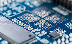
Surface Mount Technology (SMT) is a method of mounting electronic components directly onto the surface of PCBs. Unlike traditional through-hole technology, where components are inserted into holes drilled in the board and soldered on the opposite side, SMT allows for a more compact design. Components used in SMT are typically smaller and lighter, making it possible to create denser circuit layouts. This technology has become the standard in modern electronics manufacturing due to its many advantages.
Advantages of SMT in PCB Assembly
1. Increased Component Density
One of the most significant benefits of SMT is its ability to accommodate higher component density on PCBs. By eliminating the need for holes, manufacturers can place components closer together. This not only saves space but also allows for more complex circuit designs that can support advanced functionalities.
2. Reduced Manufacturing Costs
SMT contributes to lower manufacturing costs in several ways:
- Less Material Waste: The absence of drilled holes reduces material waste during production.
- Fewer Components: Smaller components often mean fewer parts are needed to achieve the same functionality.
- Automated Assembly: SMT processes are highly compatible with automation, which reduces labor costs and increases production speed.
3. Enhanced Performance
The performance of electronic devices can be significantly improved through SMT. The shorter electrical paths created by surface-mounted components reduce signal loss and interference, which is particularly important in high-frequency applications. Additionally, SMT allows for better thermal management due to improved heat dissipation from the smaller components.
4. Improved Reliability
SMT enhances the reliability of electronic devices. The solder joints created during the assembly process are generally stronger and more resistant to mechanical stress compared to through-hole connections. This durability is crucial for devices that experience vibrations or thermal cycling.
5. Flexibility in Design
With SMT, designers have greater flexibility in circuit layout and design. The ability to use a variety of component types and sizes enables engineers to innovate and optimize their designs without being constrained by traditional assembly methods.
The SMT Assembly Process
Understanding how SMT works requires a closer look at the assembly process itself, which typically involves several key steps:
1. Design and Layout
The first step in the SMT process is designing the PCB layout using specialized software. Engineers must consider component placement, trace routing, and electrical performance during this phase.
2. Solder Paste Application
Once the design is finalized, solder paste is applied to specific areas of the PCB where components will be placed. This paste is a mixture of solder powder and flux that helps create strong connections when heated.
3. Component Placement
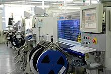
After applying solder paste, components are placed on the board using automated pick-and-place machines. These machines accurately position each component on the designated pads coated with solder paste.
4. Reflow Soldering
Once all components are placed, the board undergoes reflow soldering. The entire assembly is heated in an oven, causing the solder paste to melt and form solid connections between the components and PCB pads.
5. Inspection and Testing
The final step involves inspecting the assembled PCBs for defects and conducting functional tests to ensure everything operates as intended. Automated optical inspection (AOI) systems are often used for this purpose.

Challenges in Implementing SMT
Despite its many advantages, implementing SMT does come with challenges:
- Complexity: The design process can be more complex due to higher component density.
- Equipment Costs: Initial investment in SMT equipment can be high.
- Thermal Management: Smaller components may require advanced thermal management solutions.
- Training Requirements: Staff may need additional training to work with new technologies and processes effectively.
Future Trends in Surface Mount Technology
As technology continues to advance, several trends are shaping the future of SMT:
1. Miniaturization
The trend toward smaller devices will drive further innovations in SMT techniques and materials, allowing manufacturers to create even more compact designs without sacrificing performance.
2. Advanced Materials
Developments in materials science will lead to new types of solder pastes and substrates that improve reliability and performance under extreme conditions.
3. Increased Automation
The integration of artificial intelligence (AI) and machine learning into manufacturing processes will enhance automation capabilities, leading to faster production times and improved quality control.
4. Sustainability Initiatives
As environmental concerns grow, manufacturers will increasingly focus on sustainable practices within SMT processes, including reducing waste and using eco-friendly materials.
Conclusion
Surface Mount Technology has fundamentally changed how PCBs are assembled, offering numerous advantages over traditional methods such as increased component density, reduced costs, enhanced performance, improved reliability, and greater design flexibility. As electronics continue to evolve towards smaller and more complex devices, understanding and leveraging SMT will be crucial for manufacturers aiming to stay competitive in a rapidly changing market.
By embracing this technology, companies can not only improve their production processes but also meet the growing demands of consumers for innovative electronic solutions.

Related Questions
1. What Are Some Common Applications of Surface Mount Technology?
Surface Mount Technology is widely used in various applications including consumer electronics like smartphones and laptops, automotive electronics, medical devices, and telecommunications equipment.
2. How Does SMT Compare with Through-Hole Technology?
SMT allows for higher component density and smaller sizes compared to through-hole technology; however, through-hole technology may still be preferred for certain applications requiring robust mechanical connections.
3. What Are the Key Considerations When Designing for SMT?
Key considerations include component placement efficiency, thermal management strategies, electrical performance requirements, and ensuring manufacturability with existing equipment.
4. What Types of Components Are Commonly Used in SMT?
Common components include resistors, capacitors, integrated circuits (ICs), diodes, connectors, and inductors—all available in surface mount formats that facilitate compact designs.
5. How Can Manufacturers Ensure Quality Control in SMT Processes?
Manufacturers can implement quality control measures such as automated optical inspection (AOI), X-ray inspection for hidden solder joints, regular maintenance of equipment, and thorough testing procedures post-assembly.


