Content Menu
● Understanding SMT Stencils and Their Role
● How Stencil Thickness Influences Solder Paste Volume
● Precision and Control Challenges with Stencil Thickness
● Aspect Ratio and Area Ratio Considerations
● Selecting Stencil Thickness Based on Component Type and Pitch
● Impact on Print Quality and Defect Rates
● Manufacturing and Material Considerations
● Best Practices for Choosing Stencil Thickness
● Emerging Trends and Future Considerations in Stencil Thickness
● Conclusion
● FAQ
>> 1. What is the typical thickness range for SMT stencils used in solder paste printing?
>> 2. How does stencil thickness affect solder paste volume?
>> 3. What are aspect ratio and area ratio in stencil design?
>> 4. Why are step stencils used in SMT printing?
>> 5. What other factors influence solder paste printing quality besides stencil thickness?
Surface Mount Technology (SMT) stencil printing is a critical step in the PCB assembly process, where solder paste is precisely deposited onto pads to enable reliable solder joints. The stencil for SMT plays a pivotal role in determining the quality and volume of solder paste applied. Among the various factors influencing stencil performance, stencil thickness is one of the most significant. This article explores how stencil thickness affects SMT solder paste printing, its impact on solder joint quality, and best practices for selecting the appropriate stencil thickness.

Understanding SMT Stencils and Their Role
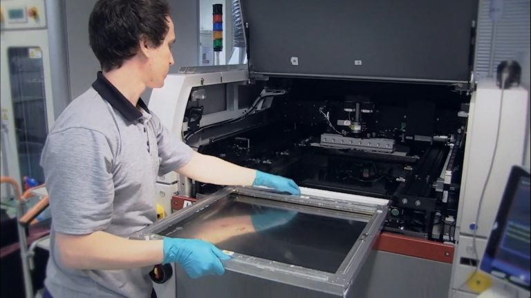
An SMT stencil is a thin metal sheet, usually made of stainless steel, with apertures that correspond to the PCB pads where solder paste is to be deposited. During printing, solder paste is forced through these apertures onto the PCB surface, ensuring precise placement and volume control. The stencil thickness directly influences the volume of solder paste deposited because it defines the depth of the aperture through which paste flows.
How Stencil Thickness Influences Solder Paste Volume
The thickness of the stencil determines the amount of solder paste deposited on each pad. A thicker stencil has deeper apertures, allowing more solder paste to be deposited, while a thinner stencil deposits less paste. This relationship is essential because different components require different solder volumes for optimal solder joints.
- Thicker Stencils: Suitable for larger components or pads requiring more solder paste. However, excessive solder paste volume can cause defects such as solder bridging, where solder connects adjacent pads unintentionally.
- Thinner Stencils: Ideal for fine-pitch components with small pads, such as 0201 or 0402 size components, where precise and minimal solder paste volume is critical to avoid bridging and ensure joint reliability.
Precision and Control Challenges with Stencil Thickness
While thicker stencils deposit more solder paste, they can reduce printing precision. Thinner stencils provide better control over the solder paste volume but may result in less stable paste release due to the roughness of aperture walls and reduced paste volume. The surface finish and manufacturing process of the stencil (e.g., laser cutting, etching) affect aperture smoothness, which in turn influences paste release and print consistency.
Aspect Ratio and Area Ratio Considerations
Two key parameters guide stencil thickness selection relative to aperture size:
- Aspect Ratio (W/T): The ratio of aperture width (W) to stencil thickness (T). A minimum acceptable aspect ratio is typically 1.5 to ensure proper paste release.
- Area Ratio: The ratio of aperture opening area to the surface area of aperture walls. A minimum of 0.66 is recommended to avoid paste sticking to aperture walls, which can cause insufficient paste deposition.
Maintaining these ratios ensures that solder paste releases cleanly from the stencil, preventing defects such as insufficient solder or bridging.
Selecting Stencil Thickness Based on Component Type and Pitch
The choice of stencil thickness depends largely on the component size, pitch, and solder volume requirements:
- For fine-pitch components (e.g., BGAs with ball pitch ≤ 0.5mm, 0201 components), stencil thicknesses of 0.08mm to 0.12mm are common to ensure precise solder paste deposition.
- For larger components or those requiring more solder paste, thicker stencils ranging from 0.15mm to 0.20mm are used.
- When a PCB has a mix of fine-pitch and larger components, step stencils with varying thicknesses in different areas can be employed to optimize solder paste volume locally.
Impact on Print Quality and Defect Rates
Stencil thickness affects not only solder paste volume but also print quality and defect rates:
- Thicker stencils may cause excessive paste deposition, leading to solder bridging, tombstoning, or solder balls.
- Thinner stencils may lead to insufficient solder paste, resulting in weak joints, solder voids, or open circuits.
- The stencil's flatness and aperture wall smoothness are critical to maintaining consistent print quality regardless of thickness.
- Other factors such as squeegee pressure, speed, angle, and solder paste rheology also interact with stencil thickness to influence print results.

Manufacturing and Material Considerations
SMT stencils are typically made from stainless steel (SUS304) with thicknesses ranging from 0.05mm to 0.30mm, depending on the application. Tight thickness tolerances (+/-1%) and flatness are essential to ensure consistent solder paste volume and accurate printing.
Coatings on stencils can improve paste release, particularly for thinner stencils where paste adhesion to aperture walls is more problematic.
Best Practices for Choosing Stencil Thickness
- Analyze the PCB component density, pad size, and pitch.
- Prioritize stencil thickness based on the smallest and most sensitive components requiring precise solder volume.
- Consider step stencils for boards with mixed component sizes to optimize solder paste volume.
- Ensure stencil manufacturing quality with smooth aperture walls and flatness.
- Maintain proper printing parameters (squeegee pressure, speed) to complement stencil thickness.
- Use IPC standards (e.g., IPC7525) as guidelines for aspect and area ratios to avoid printing defects.
Emerging Trends and Future Considerations in Stencil Thickness
As SMT technology advances, the demand for smaller, more complex components continues to grow. This trend drives the need for even thinner and more precisely manufactured stencils. Innovations in stencil materials, coatings, and manufacturing techniques are enabling better control over solder paste deposition, reducing defects, and improving yield. Additionally, the integration of automated inspection and printing systems is helping to optimize stencil usage and maintenance, ensuring consistent performance throughout production runs.
Conclusion
Stencil thickness is a fundamental factor affecting SMT solder paste printing quality and solder joint reliability. It governs the volume of solder paste deposited, influencing the risk of defects such as bridging or insufficient solder. Selecting the appropriate stencil thickness requires balancing component size, pitch, and solder volume needs while considering manufacturing quality and printing process parameters. Employing the right stencil thickness and design optimizations like step stencils can significantly improve print consistency, yield, and overall PCB assembly quality.

FAQ
1. What is the typical thickness range for SMT stencils used in solder paste printing?
The typical thickness range for SMT stencils is between 0.05mm and 0.15mm for solder paste printing, with thicker stencils (up to 0.30mm) used for other applications like red glue.
2. How does stencil thickness affect solder paste volume?
Stencil thickness directly affects the volume of solder paste deposited; thicker stencils deposit more paste due to deeper apertures, while thinner stencils deposit less paste, allowing for more precise control especially for fine-pitch components.
3. What are aspect ratio and area ratio in stencil design?
Aspect ratio is the ratio of aperture width to stencil thickness (minimum 1.5), and area ratio is the ratio of aperture opening area to the surface area of aperture walls (minimum 0.66). Both ratios ensure proper solder paste release from the stencil.
4. Why are step stencils used in SMT printing?
Step stencils have varying thicknesses in different areas to accommodate components with different solder paste volume requirements on the same PCB, optimizing paste deposition and print quality.
5. What other factors influence solder paste printing quality besides stencil thickness?
Factors include aperture shape and smoothness, squeegee hardness and pressure, printing speed and angle, solder paste rheology and particle size, and PCB flatness and registration.


