Content Menu
● Understanding the Role of the SMT Stencil in Solder Paste Printing
● How SMT Stencils Enhance Solder Paste Printing
>> Precision and Accuracy in Paste Deposition
>> Consistency and Repeatability
>> Increased Efficiency and Throughput
>> Flexibility for Complex and Fine-Pitch Components
>> Improved Quality Control and Yield
>> Cost Savings and Material Optimization
● Types of SMT Stencils and Their Impact on Printing
>> Frameless SMT Stencils
>> Framed SMT Stencils
>> Step and Nano-Coated Stencils
● Technological Advancements in SMT Stencil Printing
>> Automated SMT Stencil Printers
>> Controlled Separation and Environmental Control
>> Real-Time Inspection and Feedback
● Best Practices for Using SMT Stencils in Solder Paste Printing
>> Proper Stencil Selection
>> Regular Cleaning and Maintenance
>> Correct Squeegee Pressure and Speed
>> Environmental Controls
>> Inspection and Process Monitoring
● Challenges and Solutions in SMT Stencil Printing
>> Aperture Clogging
>> Paste Smearing and Bridging
>> Warping and Tension Loss in Stencils
>> Handling Fine-Pitch and High-Density PCBs
● Future Trends in SMT Stencil Technology
>> Advanced Materials
>> Integration with Industry 4.0
>> Enhanced Coatings and Surface Treatments
>> Miniaturization and Microelectronics
● Conclusion
● FAQ
>> 1. What is the main function of a stencil in SMT solder paste printing?
>> 2. How does stencil thickness affect solder paste printing?
>> 3. What advantages do nano-coated SMT stencils provide?
>> 4. Why is precise alignment important in SMT stencil printing?
>> 5. Can SMT stencil printing be used for both prototype and mass production?
Surface Mount Technology (SMT) has revolutionized the electronics manufacturing industry by enabling efficient, precise, and high-density assembly of printed circuit boards (PCBs). At the heart of this process lies the solder paste printing stage, which is critical for ensuring reliable electrical connections between components and the PCB. The SMT stencil plays a pivotal role in this stage, directly impacting the quality, efficiency, and yield of the assembly process. This article explores how an SMT stencil improves solder paste printing, detailing its functions, types, benefits, and the technological advancements that enhance its performance.

Understanding the Role of the SMT Stencil in Solder Paste Printing
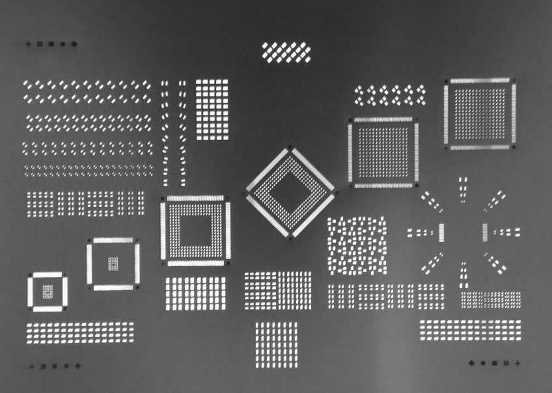
An SMT stencil is a thin sheet, typically made of stainless steel or nickel alloy, with precisely laser-cut apertures that correspond to the solder pads on a PCB. Its primary function is to facilitate the accurate deposition of solder paste onto these pads during the printing process. The stencil acts as a mask, allowing solder paste to pass only through the apertures and onto the PCB surface, ensuring that the right amount of solder paste is applied exactly where it is needed.
The solder paste itself is a mixture of solder powder and flux, designed to temporarily hold components in place and create strong solder joints once reflowed. The stencil's precision in controlling paste volume and placement is essential to avoid defects such as solder bridging, insufficient solder, or misaligned components, which can compromise the electrical and mechanical integrity of the finished product.
How SMT Stencils Enhance Solder Paste Printing
Precision and Accuracy in Paste Deposition
One of the most significant ways an SMT stencil improves solder paste printing is by ensuring precise and uniform deposition of solder paste on the PCB pads. The apertures in the stencil are engineered to match the size and shape of the pads exactly, which controls the volume of solder paste deposited. This precision minimizes the risk of solder bridging between adjacent pads and ensures consistent solder joint quality across the board.
Advanced manufacturing techniques, such as laser cutting and electro-polishing, produce smooth aperture walls that help in the clean release of solder paste. Some modern stencils are coated with nano-coatings that repel solder paste from the aperture walls, further improving paste release and reducing defects.
Consistency and Repeatability
Using an SMT stencil standardizes the solder paste application process, which is crucial for maintaining consistency across multiple PCBs, especially in high-volume production. The stencil ensures that every board receives the same amount of solder paste in the exact locations, reducing variability caused by manual application methods. This repeatability enhances overall product quality and reduces the incidence of rework or scrap.
Increased Efficiency and Throughput
SMT stencils enable simultaneous printing of solder paste on multiple pads, significantly speeding up the assembly process compared to manual solder paste application. The stencil printing process is often automated with stencil printers that use precise alignment systems and controlled squeegee pressure to apply solder paste quickly and accurately. This automation increases throughput, allowing manufacturers to meet tight production schedules and reduce labor costs.
Flexibility for Complex and Fine-Pitch Components
Modern electronics often feature fine-pitch components with very small and closely spaced pads. SMT stencils are designed to accommodate these challenging layouts by offering finely tuned aperture designs and thicknesses. Step stencils, for example, have varying thicknesses in different areas to optimize paste volume for both fine-pitch and larger pads on the same PCB.
This adaptability ensures that solder paste printing meets the demands of advanced PCB designs without sacrificing quality or reliability.
Improved Quality Control and Yield
The quality of solder paste printing directly impacts the yield of the PCB assembly process. Poor paste deposition can lead to defects such as solder bridges, insufficient solder joints, tombstoning, or component misalignment. By using an SMT stencil, manufacturers can achieve higher first-pass yields due to more accurate and consistent solder paste application.
Some advanced stencil printing systems include real-time inspection capabilities that monitor paste deposition quality, allowing immediate correction of printing parameters and preventing defective boards from advancing to subsequent assembly stages.
Cost Savings and Material Optimization
Accurate solder paste deposition reduces material waste by limiting excess paste usage and minimizing the need for rework. The stencil ensures that only the necessary amount of solder paste is applied, which lowers material costs and reduces the environmental impact of manufacturing. Additionally, higher yields and fewer defects translate to lower overall production costs.
Types of SMT Stencils and Their Impact on Printing
Frameless SMT Stencils
Frameless stencils are thin, flexible sheets without a supporting frame, often used for prototypes or small production runs. They are cost-effective and easy to store but require careful handling to maintain tension and flatness during printing. While suitable for less demanding applications, frameless stencils may offer less stability and repeatability compared to framed versions.
Framed SMT Stencils
Framed stencils are mounted on rigid frames that provide stability and tension during printing. This stability improves print consistency and is ideal for high-volume manufacturing where repeatability is critical. The frame also simplifies handling and alignment, reducing setup time and operator errors.
Step and Nano-Coated Stencils
Step stencils have varying thicknesses to optimize paste volume for different pad sizes on a PCB. Nano-coated stencils feature a hydrophobic coating that improves solder paste release from aperture walls, reducing defects and improving print quality. These advanced stencil types are essential for fine-pitch components and complex PCB designs.

Technological Advancements in SMT Stencil Printing
Automated SMT Stencil Printers
Modern SMT stencil printers incorporate sophisticated features such as vision systems for precise alignment, automated paste dispensing, and controlled squeegee pressure and speed. These features ensure optimal paste transfer and reduce variability caused by manual processes.
Controlled Separation and Environmental Control
The speed and method by which the stencil separates from the PCB after printing affect paste release quality. Automated printers control this separation to achieve clean, well-defined paste deposits. Additionally, maintaining optimal temperature and humidity during printing preserves solder paste properties, enhancing print consistency.
Real-Time Inspection and Feedback
Some SMT stencil printing systems include inline inspection capabilities that detect printing defects immediately. This feedback allows operators to adjust parameters on the fly, improving yield and reducing waste.
Best Practices for Using SMT Stencils in Solder Paste Printing
Proper Stencil Selection
Choosing the right stencil in SMT is critical for optimizing solder paste printing. Factors such as stencil thickness, aperture design, and material must align with the PCB design and component requirements. For example, fine-pitch components require thinner stencils with precisely shaped apertures, while larger pads may benefit from thicker stencil areas or step stencils.
Regular Cleaning and Maintenance
Stencil cleanliness directly affects solder paste release and print quality. Residual paste or contaminants can clog apertures, causing inconsistent paste deposition. Regular cleaning using appropriate solvents and ultrasonic cleaning systems ensures the stencil remains in optimal condition, prolonging its lifespan and maintaining print quality.
Correct Squeegee Pressure and Speed
Applying the right squeegee pressure and speed during printing is essential to achieve uniform paste deposition. Excessive pressure can cause paste smearing or stencil damage, while insufficient pressure may lead to incomplete paste transfer. Automated printers help control these parameters precisely for consistent results.
Environmental Controls
Solder paste properties are sensitive to temperature and humidity. Maintaining a controlled environment during stencil printing helps preserve paste viscosity and tackiness, ensuring proper paste transfer and adhesion. This control reduces variability and improves overall print quality.
Inspection and Process Monitoring
Implementing inspection systems to monitor solder paste deposition after printing helps identify defects early. Automated optical inspection (AOI) and paste inspection systems provide feedback for process adjustments, reducing defects and improving yield.
Challenges and Solutions in SMT Stencil Printing
Aperture Clogging
Aperture clogging occurs when solder paste dries or accumulates in stencil apertures, leading to incomplete paste deposits. This issue is mitigated by frequent cleaning, using stencil coatings that reduce paste adhesion, and optimizing paste formulation and printing parameters.
Paste Smearing and Bridging
Improper stencil design, incorrect squeegee settings, or misalignment can cause paste smearing or bridging between pads. Using well-designed apertures, precise alignment systems, and controlled printing parameters helps prevent these defects.
Warping and Tension Loss in Stencils
Frameless stencils may warp or lose tension, affecting print consistency. Using framed stencils or tensioning systems maintains flatness and stability during printing, ensuring uniform paste deposition.
Handling Fine-Pitch and High-Density PCBs
As PCB designs become more complex, stencil apertures shrink and become more densely packed. Advanced laser cutting technology, step stencils, and nano-coatings address these challenges by improving aperture accuracy and paste release.
Future Trends in SMT Stencil Technology
Advanced Materials
Research into new materials such as ultra-thin nickel stencils and composite alloys aims to improve stencil durability, reduce wear, and enhance paste release properties.
Integration with Industry 4.0
The integration of SMT stencil printing with Industry 4.0 concepts, including IoT connectivity, data analytics, and machine learning, enables smarter process control and predictive maintenance, further improving print quality and manufacturing efficiency.
Enhanced Coatings and Surface Treatments
Development of next-generation coatings that provide superior anti-stick properties and resistance to wear will extend stencil life and improve print consistency.
Miniaturization and Microelectronics
As electronic devices continue to shrink, SMT stencil technology will evolve to accommodate increasingly fine-pitch components and complex PCB layouts, ensuring reliable solder paste printing at microscopic scales.
Conclusion
The SMT stencil is a fundamental component in the solder paste printing process, directly influencing the quality, efficiency, and cost-effectiveness of PCB assembly. By enabling precise, consistent, and controlled deposition of solder paste, the stencil helps manufacturers achieve reliable solder joints, reduce defects, and increase production throughput. Advances in stencil materials, design, and printing technology continue to enhance these benefits, supporting the growing complexity and miniaturization of modern electronic devices. Integrating high-quality SMT stencils and automated printing systems is essential for any manufacturer aiming to maintain competitive advantage and deliver superior electronic products.

FAQ
1. What is the main function of a stencil in SMT solder paste printing?
The main function of an SMT stencil is to accurately deposit the correct amount of solder paste onto the PCB pads by allowing paste to pass only through precisely cut apertures that align with the pads, ensuring consistent and reliable solder joints.
2. How does stencil thickness affect solder paste printing?
Stencil thickness determines the volume of solder paste deposited. Thicker stencils deposit more paste, suitable for larger pads, while thinner stencils are used for fine-pitch components to prevent excessive paste that can cause bridging. Step stencils with varying thicknesses optimize paste volume for different pad sizes on the same PCB.
3. What advantages do nano-coated SMT stencils provide?
Nano-coated stencils have hydrophobic coatings that repel solder paste from aperture walls, improving paste release and reducing defects such as smearing or insufficient paste. This leads to cleaner prints and higher yield rates.
4. Why is precise alignment important in SMT stencil printing?
Precise alignment ensures that solder paste is deposited exactly on the PCB pads, preventing misalignment that can cause solder bridges, open joints, or component placement issues. Automated vision systems in stencil printers enhance alignment accuracy.
5. Can SMT stencil printing be used for both prototype and mass production?
Yes, frameless stencils are often used for prototypes due to their flexibility and cost-effectiveness, while framed stencils provide the stability and repeatability required for mass production. Modern stencil printing systems can be adapted for both scenarios.


