Content Menu
● The Evolution of PCB Inspection
● The Working Principle of 3D PCB SMT Inspection Machines
>> Data Acquisition
>> Image Processing and Analysis
● Types of Defects Detected by 3D PCB SMT Inspection Machines
● Advanced Technologies in 3D PCB SMT Inspection Machines
>> Phase Modulation Profile (PMP) Technology
>> Programmable Structure Grating (PSLM)
● The Inspection Process
● Benefits of 3D PCB SMT Inspection Machines
● Challenges and Limitations
● Future Trends in PCB Inspection
● Conclusion
● FAQ
>> 1. What is the difference between 2D and 3D PCB inspection?
>> 2. How accurate are 3D PCB SMT inspection machines?
>> 3. Can 3D PCB SMT inspection machines replace human inspectors entirely?
>> 4. How long does it take to inspect a PCB using a 3D SMT inspection machine?
>> 5. What types of defects can a máy kiểm tra pcb smt detect?
● Citations:
In the rapidly evolving world of electronics manufacturing, quality control is paramount. One of the most critical stages in the production of printed circuit boards (PCBs) is the inspection process. As technology advances, so do the methods used to ensure the highest standards of quality in PCB assembly. Among these advanced techniques, 3D PCB SMT (Surface Mount Technology) inspection machines have emerged as a game-changer. These sophisticated devices, also known as máy kiểm tra pcb smt in Vietnamese, have revolutionized the way we detect defects and maintain quality in PCB production.

The Evolution of PCB Inspection
Before delving into the intricacies of 3D PCB SMT inspection machines, it's essential to understand the context of their development. Traditionally, PCB inspection was a manual process, relying on the keen eyes of skilled technicians. However, as PCBs became more complex and production volumes increased, this method proved to be time-consuming and prone to human error.
The introduction of Automated Optical Inspection (AOI) systems marked a significant leap forward. These 2D systems could rapidly scan PCBs for surface-level defects, dramatically improving inspection speed and accuracy[7]. However, as PCB designs became more intricate, with components shrinking in size and increasing in density, the limitations of 2D inspection became apparent.
This is where 3D PCB SMT inspection machines, or máy kiểm tra pcb smt, come into play. These advanced systems combine the speed of automation with the ability to analyze the three-dimensional aspects of PCB assembly, offering a level of inspection that was previously unattainable.
The Working Principle of 3D PCB SMT Inspection Machines
Data Acquisition
The first step in the 3D PCB SMT inspection process is data acquisition. This phase involves capturing detailed images and creating a three-dimensional profile of the PCB under inspection. Here's how it works:
1. Multiple Camera Imaging: The PCB is photographed from various angles using high-resolution cameras. These images provide a comprehensive view of the board's surface and components[1].
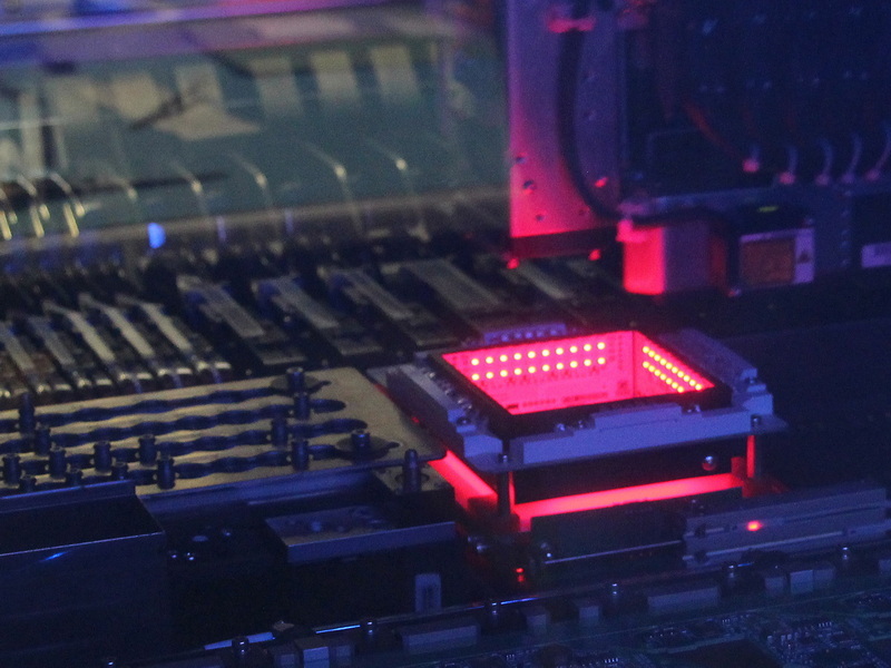
2. Structured Light Projection: Patterns of light are projected onto the PCB surface. By analyzing how these patterns deform when projected onto three-dimensional objects, the system can create a detailed 3D map of the board[1].
3. Laser Triangulation: In some systems, laser beams are used to measure the height and profile of components with high precision[1].
4. Shadow Moiré Technology: This technique uses the interference patterns created by a reference grating and its shadow on the PCB to measure surface topography accurately[1].
The combination of these techniques allows the 3D PCB SMT inspection machine (máy kiểm tra pcb smt) to gather a wealth of data about the PCB's physical characteristics, far beyond what is possible with traditional 2D inspection methods.
Image Processing and Analysis
Once the raw data is acquired, the 3D PCB SMT inspection system processes and analyzes it to identify potential defects. This stage involves several sophisticated algorithms and techniques:
1. Image Enhancement: Raw images are processed to improve contrast, reduce noise, and highlight features of interest[1].
2. 3D Reconstruction: The system combines data from multiple sources to create a detailed 3D model of the PCB[1].
3. Feature Extraction: Key features such as component edges, solder joints, and pad locations are identified and isolated for further analysis[1].
4. Pattern Matching: The observed features are compared against a database of known good examples or CAD data to identify discrepancies[1].
5. Defect Classification: Any anomalies detected are classified into specific types of defects based on predefined criteria[1].
Types of Defects Detected by 3D PCB SMT Inspection Machines
The advanced capabilities of 3D PCB SMT inspection machines (máy kiểm tra pcb smt) allow them to detect a wide range of defects that might be missed by 2D systems or human inspectors. Some of the key defects these machines can identify include:
1. Component Placement Issues: The machine can detect if components are missing, misaligned, or incorrectly oriented[5].
2. Solder Joint Defects: It can identify problems such as insufficient solder, excess solder, bridging between joints, and cold or dry joints[5].
3. Lifted Leads: The 3D imaging capabilities allow the machine to detect lifted or bent leads on components, which might not be visible from a top-down view[5].
4. Coplanarity Issues: For components like BGAs (Ball Grid Arrays) and QFPs (Quad Flat Packages), the machine can verify that all leads or balls are at the correct height[5].
5. Solder Paste Defects: When used for solder paste inspection, the machine can detect issues such as insufficient paste, excess paste, or smearing[3].
6. Foreign Object Detection: The system can identify any foreign objects or contaminants on the PCB surface.
7. Component Polarity: It can verify that polarized components are oriented correctly[5].
8. Tombstoning: The machine can detect when small components have been lifted at one end due to uneven solder reflow, a defect known as tombstoning[5].

Advanced Technologies in 3D PCB SMT Inspection Machines
Phase Modulation Profile (PMP) Technology
One of the most advanced technologies used in modern 3D PCB SMT inspection machines is Phase Modulation Profile (PMP) technology. This method offers several advantages over older laser-based systems:
1. Higher Resolution: PMP technology provides a detection resolution of 0.37 microns, which is significantly higher than laser-based systems[3].
2. Multiple Sampling: The system samples each solder paste area 8 times, ensuring high repeatability and accuracy[3].
3. Color Adaptability: Unlike laser systems, PMP technology is not affected by the color of the PCB, making it more versatile[3].
4. Reduced Vibration Impact: Some PMP systems use a "stop-and-go" approach, where sampling is done when the machine is stationary, minimizing the impact of vibration on the measurements[3].
Programmable Structure Grating (PSLM)
Another cutting-edge technology used in some 3D PCB SMT inspection machines is Programmable Structure Grating (PSLM). This technology offers several benefits:
1. Software Control: PSLM allows for software control of the structure grating movement, eliminating the need for mechanical devices like piezoelectric ceramic motors[3].
2. Reduced Maintenance: By reducing mechanical wear, PSLM technology lowers maintenance costs for users[3].
3. Enhanced Detection Capability: The combination of PSLM with PMP technology significantly improves the detection capabilities of the máy kiểm tra pcb smt[3].
The Inspection Process
The inspection process using a 3D PCB SMT inspection machine typically follows these steps:
1. Board Loading: The PCB is loaded into the machine, either manually or automatically in a production line setting.
2. Alignment and Calibration: The machine aligns the board and calibrates its cameras and lighting systems.
3. Data Acquisition: The machine captures multiple images and 3D data of the PCB.
4. Image Processing: The captured data is processed and analyzed using sophisticated algorithms.
5. Defect Detection: The system identifies any anomalies or defects based on predefined criteria.
6. Reporting: A detailed report is generated, highlighting any detected defects and their locations on the board.
7. Decision Making: Based on the report, decisions are made about whether the board passes inspection or needs rework.
Benefits of 3D PCB SMT Inspection Machines
The adoption of 3D PCB SMT inspection machines (máy kiểm tra pcb smt) offers numerous benefits to electronics manufacturers:
1. Improved Accuracy: 3D inspection can detect defects that might be missed by 2D systems or human inspectors.
2. Increased Speed: These machines can inspect PCBs much faster than manual inspection, improving production throughput.
3. Consistency: Automated inspection eliminates variations that can occur with human inspectors, ensuring consistent quality standards.
4. Data Collection: The machines generate detailed data that can be used for process improvement and traceability.
5. Cost Reduction: By catching defects early in the production process, these machines can significantly reduce rework costs and improve overall yield.
6. Handling Complex Designs: As PCBs become more complex and densely populated, 3D inspection becomes increasingly necessary to ensure quality.
Challenges and Limitations
While 3D PCB SMT inspection machines offer significant advantages, they also come with some challenges:
1. Initial Cost: These machines represent a significant capital investment for manufacturers.
2. Programming Time: Setting up the inspection parameters for each new PCB design can be time-consuming.
3. False Positives: Sometimes, the machines may flag issues that turn out to be acceptable variations, requiring human verification.
4. Maintenance and Calibration: Regular maintenance and calibration are necessary to ensure the machine's accuracy over time.
5. Training Requirements: Operators need specialized training to effectively use and interpret the results from these machines.
Future Trends in PCB Inspection
As technology continues to evolve, we can expect to see further advancements in 3D PCB SMT inspection machines:
1. Artificial Intelligence Integration: AI and machine learning algorithms are likely to play a larger role in defect detection and classification.
2. Increased Automation: Future systems may be more fully integrated into automated production lines, with less need for human intervention.
3. Higher Resolution: We can expect continued improvements in imaging technology, allowing for even more precise measurements.
4. Expanded Inspection Capabilities: Future machines may be able to inspect an even wider range of components and defect types.
5. Integration with Other Systems: Inspection data may be more tightly integrated with other manufacturing systems for improved process control.
Conclusion
3D PCB SMT inspection machines, or máy kiểm tra pcb smt, represent a significant leap forward in electronics manufacturing quality control. By combining advanced imaging technologies with sophisticated data analysis, these machines offer unprecedented accuracy and speed in detecting PCB assembly defects. As PCBs continue to become more complex and miniaturized, the role of these inspection systems will only grow in importance.
While challenges exist, the benefits of improved quality, reduced costs, and increased production efficiency make 3D PCB SMT inspection machines an invaluable tool for modern electronics manufacturers. As technology continues to evolve, we can expect these systems to become even more sophisticated, further enhancing their capabilities and cementing their place as a crucial component in the pursuit of perfect PCB assembly.

FAQ
1. What is the difference between 2D and 3D PCB inspection?
2D PCB inspection uses top-down imaging to detect surface-level defects, while 3D PCB inspection uses multiple cameras and structured light to create a three-dimensional model of the PCB. This allows 3D inspection to detect issues like component height, coplanarity, and solder joint quality that may not be visible from a top-down view.
2. How accurate are 3D PCB SMT inspection machines?
3D PCB SMT inspection machines can achieve very high levels of accuracy. For example, systems using Phase Modulation Profile (PMP) technology can achieve a resolution of 0.37 microns, which is significantly more precise than human inspection or older inspection technologies.
3. Can 3D PCB SMT inspection machines replace human inspectors entirely?
While 3D PCB SMT inspection machines are highly accurate and efficient, they typically don't replace human inspectors entirely. Human expertise is still valuable for interpreting results, handling edge cases, and making final decisions on borderline defects. However, these machines significantly reduce the workload on human inspectors and improve overall inspection accuracy.
4. How long does it take to inspect a PCB using a 3D SMT inspection machine?
The inspection time can vary depending on the size and complexity of the PCB, as well as the specific machine being used. However, 3D SMT inspection machines are generally much faster than manual inspection. Some advanced systems can inspect several boards per minute in a production line setting.
5. What types of defects can a máy kiểm tra pcb smt detect?
A máy kiểm tra pcb smt (3D PCB SMT inspection machine) can detect a wide range of defects, including component misalignment, missing components, solder joint issues (like insufficient or excess solder), lifted leads, coplanarity problems, foreign object detection, and even issues with solder paste application if used before component placement.
Citations:
[1] https://www.raypcb.com/how-does-3d-automated-optical-inspection-work-in-the-pcb-assembly-process/
[2] https://patents.google.com/patent/CN112040669B/zh
[3] https://www.ipcb.com/pcba-tech/8707.html
[4] https://baike.baidu.com/item/%E7%94%B5%E5%AD%90%E7%BB%84%E8%A3%85%E6%8A%80%E6%9C%AF%E4%B8%93%E4%B8%9A%E8%8B%B1%E8%AF%AD/12086345
[5] https://www.youtube.com/watch?v=xctsO8qUpDw
[6] https://smtnet.com/library/index.cfm?fuseaction=browse_articles&start_at=296
[7] https://en.wikipedia.org/wiki/Automated_optical_inspection
[8] https://patents.google.com/patent/CN101257788A/zh


