Content Menu
● What are SMT Packages?
● Impact of SMT Packages on PCB Performance
>> 1. Size and Weight Reduction
>> 2. Electrical Performance
>> 3. Manufacturability
>> 4. Reliability
● Design Considerations for SMT Packages
>> 1. Pad Design
>> 2. Trace Width and Length
>> 3. Thermal Management
>> 4. Component Placement
>> 5. Testing and Validation
● Challenges Associated with SMT Packages
>> 1. Complexity in Design
>> 2. Solder Joint Reliability
>> 3. Cost Considerations
● Future Trends in SMT Packages
>> 1. Miniaturization
>> 2. Advanced Materials
>> 3. Integration of Components
>> 4. Sustainability Considerations
● Conclusion
● FAQ
>> 1. What are the advantages of using SMT over traditional through-hole technology?
>> 2. How do I choose the right SMT package for my application?
>> 3. What role does thermal management play in PCB design with SMT components?
>> 4. How can I ensure reliability when using SMT packages?
>> 5. What future trends should I be aware of regarding SMT packaging?
Surface Mount Technology (SMT) has revolutionized the landscape of electronics manufacturing, allowing for smaller, lighter, and more efficient printed circuit boards (PCBs). As the demand for compact and high-performance electronic devices continues to grow, understanding how SMT packages affect PCB performance becomes crucial. This article delves into the intricacies of SMT packages, their impact on PCB performance, design considerations, and future trends in the industry.

What are SMT Packages?
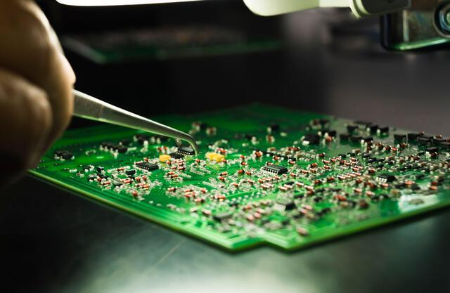
Surface Mount Technology (SMT) refers to a method of mounting electronic components directly onto the surface of PCBs. Unlike traditional through-hole technology, where components are inserted into holes drilled in the board, SMT packages are soldered onto pads on the board's surface. This technology offers several advantages, including reduced space requirements and improved electrical performance.
SMT packages come in various shapes and sizes, including:
- Chip Resistors: Small resistors used in various applications.
- Chip Capacitors: Essential for filtering and energy storage.
- Integrated Circuits (ICs): Complex components that can perform multiple functions.
- Transistors: Used for amplification and switching.
- Connectors: Allowing for external connections.
The choice of SMT package can significantly influence the overall performance of a PCB.
Impact of SMT Packages on PCB Performance
1. Size and Weight Reduction
One of the most significant advantages of using SMT packages is their compact size. This reduction in size allows for:
- Higher Component Density: More components can be placed on a single board, leading to increased functionality without enlarging the device footprint. This is particularly beneficial in consumer electronics where space is at a premium.
- Lightweight Designs: Reducing the weight of electronic devices is critical in applications such as mobile phones and laptops where portability is essential. Lightweight designs can also lead to lower shipping costs and easier handling during assembly.
2. Electrical Performance
SMT packages can enhance electrical performance through:
- Shorter Interconnects: The proximity of components reduces the length of traces, minimizing inductance and capacitance effects that can degrade signal integrity. This is especially important in high-frequency applications where signal integrity is paramount.
- Improved Thermal Management: Many SMT packages are designed to dissipate heat more effectively than traditional through-hole components. This is particularly important in high-power applications where overheating can lead to failure. Enhanced thermal management helps maintain optimal operating conditions for sensitive components.
3. Manufacturability
The use of SMT packages simplifies the manufacturing process:
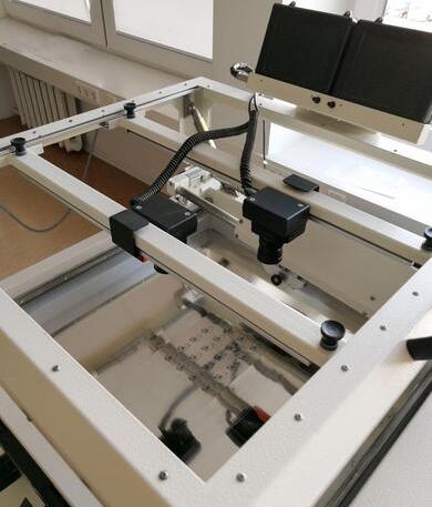
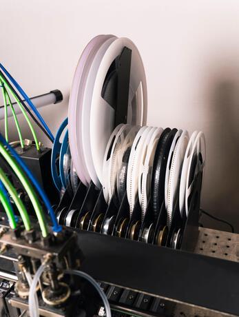
- Automated Assembly: SMT components can be placed on PCBs using pick-and-place machines, increasing production speed and reducing labor costs. Automation also minimizes human error during assembly.
- Reflow Soldering: This technique allows for uniform soldering across all components, reducing defects compared to manual soldering methods. Reflow soldering provides better control over solder joint quality and consistency.
4. Reliability
Reliability is a critical factor in PCB performance. SMT packages contribute to reliability through:
- Strain Relief: The solder joints created during reflow soldering provide better mechanical support than through-hole joints, which can be prone to cracking under stress. This is particularly important in applications subject to vibration or thermal cycling.
- Resistance to Environmental Factors: Many SMT packages are designed to withstand harsh conditions, including moisture and temperature fluctuations, enhancing long-term reliability. The encapsulation materials used in SMT packages often provide additional protection against environmental stressors.
Design Considerations for SMT Packages
When designing PCBs with SMT packages, several factors must be considered to optimize performance:
1. Pad Design
The pad layout is crucial for ensuring proper solder joints. Designers must consider:
- Pad Size and Shape: The dimensions should match the package specifications to ensure adequate solder coverage. Incorrect pad sizes can lead to insufficient solder joints or excessive solder that may cause bridging.
- Pad Spacing: Adequate spacing between pads prevents solder bridging during reflow. Designers should follow IPC standards for pad spacing based on component size and type.
2. Trace Width and Length
The width and length of traces connecting SMT components affect signal integrity:
- Trace Width Calculation: Designers should calculate trace widths based on current carrying capacity to prevent overheating. This involves considering factors such as ambient temperature and allowable temperature rise.
- Minimizing Trace Lengths: Keeping traces short reduces resistance and inductance, improving overall circuit performance. Shorter traces also reduce susceptibility to noise interference from adjacent signals.

3. Thermal Management
Effective thermal management strategies are essential:
- Thermal Vias: Incorporating thermal vias can help dissipate heat away from critical components. These vias allow heat to transfer from one layer of a multi-layer PCB to another, enhancing overall heat dissipation.
- Copper Pour Areas: Utilizing larger copper areas can aid in heat dissipation by spreading heat across a larger surface area. This technique can be particularly effective when combined with thermal vias.
4. Component Placement
Strategic component placement enhances performance:
- Critical Signal Paths: Place high-speed components close together to minimize trace lengths. This reduces signal degradation caused by longer interconnects.
- Power Distribution: Ensure that power supply components are adequately spaced to reduce noise coupling between them. Proper placement also helps balance current distribution across the PCB.
5. Testing and Validation
After designing PCBs with SMT packages, thorough testing is essential:
- Functional Testing: Validate that all components operate as intended under various conditions. Functional tests should simulate real-world operating scenarios to identify potential failures early.
- Thermal Testing: Assess how well the PCB manages heat under load conditions. Thermal imaging techniques can help identify hot spots that may require additional cooling measures.
Challenges Associated with SMT Packages
Despite their numerous advantages, using SMT packages also presents certain challenges that designers must address:
1. Complexity in Design
The compact nature of SMT packages requires careful planning during the design phase:
- Increased Design Complexity: As component density increases, managing routing becomes more complex. Designers must balance functionality with manufacturability while adhering to design rules.
2. Solder Joint Reliability
While SMT offers improved mechanical support through solder joints, these joints can still fail under certain conditions:
- Thermal Cycling Effects: Repeated heating and cooling cycles can lead to fatigue in solder joints over time, especially if not properly designed or if materials are not suited for such conditions.
3. Cost Considerations
While automated assembly reduces labor costs, other factors may influence overall costs:
- Component Costs: Some advanced SMT packages may have higher initial costs due to their complexity or specialized materials.
- Testing Costs: Comprehensive testing protocols may increase upfront investment but are essential for ensuring long-term reliability.
Future Trends in SMT Packages
As technology advances, several trends are shaping the future of SMT packages:
1. Miniaturization
The push for smaller devices will continue to drive innovations in SMT package design:
- Smaller Components with Higher Functionality: Manufacturers are developing even smaller components without sacrificing performance or functionality—this trend will enable even more compact designs across various applications.
2. Advanced Materials
New materials that offer better thermal conductivity or electrical performance will emerge:
- High-Density Interconnects (HDI): These technologies allow for finer traces and smaller pads, enabling higher component densities while maintaining signal integrity.
3. Integration of Components
The trend towards integrating multiple functions into a single package will continue:
- System-in-Package (SiP): SiP technology combines multiple integrated circuits into one package, reducing space requirements while enhancing functionality—this approach is gaining popularity in mobile devices and IoT applications.
4. Sustainability Considerations
As environmental concerns grow, manufacturers will focus on developing eco-friendly materials and processes for SMT packaging that reduce waste and energy consumption during production:
- Recyclable Materials: Innovations aimed at using recyclable materials will help reduce environmental impact while maintaining performance standards.
Conclusion
In summary, SMT packages play a pivotal role in determining PCB performance. Their compact size allows for higher component density while enhancing electrical performance through shorter interconnects and improved thermal management. As technology evolves, understanding how these packages affect PCB design becomes increasingly important for engineers seeking to create reliable and efficient electronic devices. By considering factors such as pad design, trace width, thermal management, component placement, and thorough testing, designers can maximize the benefits of SMT technology in their applications.
With ongoing advancements in materials and integration techniques, the future looks promising for SMT packages as they continue to meet the demands of modern electronics while pushing the boundaries of innovation.

FAQ
1. What are the advantages of using SMT over traditional through-hole technology?
SMT offers several advantages including reduced size and weight of PCBs, automated assembly processes leading to faster production times, improved electrical performance due to shorter interconnects, and enhanced reliability through better mechanical support at solder joints.
2. How do I choose the right SMT package for my application?
Selecting an appropriate SMT package involves considering factors such as size constraints, electrical requirements (like power rating), thermal characteristics (heat dissipation needs), and compatibility with existing manufacturing processes.
3. What role does thermal management play in PCB design with SMT components?
Thermal management is crucial as it ensures that components operate within safe temperature limits. Effective strategies include using thermal vias for heat dissipation, copper pour areas for spreading heat across surfaces, and careful placement of heat-sensitive components away from high-power areas.
4. How can I ensure reliability when using SMT packages?
To ensure reliability with SMT packages, focus on proper pad design to achieve good solder joints, minimize mechanical stress on components through strain relief techniques, select materials that withstand environmental conditions, and conduct thorough testing during development phases.
5. What future trends should I be aware of regarding SMT packaging?
Future trends include continued miniaturization of components without sacrificing performance; advancements in materials that enhance thermal conductivity; integration of multiple functions into single packages; and a growing emphasis on sustainability practices within manufacturing processes.


