Content Menu
● Understanding SMT PCB Assembly
● Key Steps in Designing a PCB for SMT Assembly
>> 1. Schematic Design
>> 2. Component Selection
>> 3. PCB Layout
>> 4. Design for Manufacturability (DFM)
>> 5. Solder Paste Considerations
>> 6. Reflow Profile Planning
● Advanced Considerations for SMT PCB Design
>> High-Density Interconnect (HDI) Techniques
>> Mixed Technology Designs
>> Flex and Rigid-Flex PCB Considerations
● The SMT Assembly Process
● Best Practices for SMT PCB Design
● Common Challenges in SMT PCB Design
● Future Trends in SMT PCB Design
● Conclusion
● FAQ
>> 1. What are the main advantages of SMT over through-hole technology?
>> 2. How do I choose the right solder paste for my SMT PCB?
>> 3. What are some common SMT component package types?
>> 4. How can I improve the thermal management of my SMT PCB design?
>> 5. What are some common SMT assembly defects and how can I prevent them in my design?
● Citations:
Designing a PCB (Printed Circuit Board) for Surface Mount Technology (SMT) assembly is a crucial step in the electronics manufacturing process. SMT has become the preferred method for assembling electronic components onto PCBs due to its efficiency, compact design capabilities, and cost-effectiveness. This article will guide you through the essential steps and considerations for designing a PCB optimized for SMT assembly.

Understanding SMT PCB Assembly
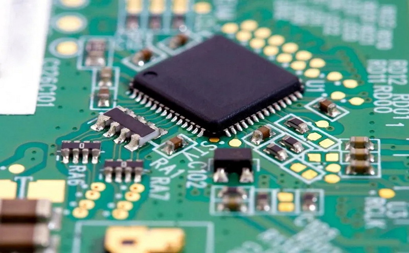
Before delving into the design process, it's important to understand what SMT PCB assembly entails. Surface Mount Technology is a method where electronic components are mounted directly onto the surface of a PCB[1]. Unlike through-hole technology, SMT doesn't require component leads to be inserted through holes in the board. This allows for more compact designs, faster assembly, and improved performance in many applications.
Key Steps in Designing a PCB for SMT Assembly
1. Schematic Design
The first step in designing a PCB for SMT assembly is creating a comprehensive schematic diagram. This serves as the blueprint for your circuit and defines how each component is connected[1]. When designing your schematic:
- Select appropriate surface-mount components from available libraries
- Ensure all connections between components (nets) are properly mapped out
- Label key signals and power distribution for easy reference
2. Component Selection
Choosing the right components is crucial for successful SMT assembly. Consider the following:
- Select components with appropriate package sizes for SMT
- Ensure components are readily available and suitable for the assembly process
- Use standard package sizes when possible to simplify the assembly process
3. PCB Layout
The PCB layout is where your schematic design is translated into a physical board layout. This stage is critical for ensuring optimal performance and manufacturability. Key considerations include:
Component Placement
- Group components based on function
- Place critical components, such as microcontrollers and power supplies, first
- Consider signal flow and minimize trace lengths for high-speed signals
- Leave adequate space between components for ease of assembly and rework
Thermal Management
- Provide sufficient copper area for heat dissipation, especially for power-intensive components
- Use thermal vias to improve heat transfer in multilayer boards
Signal Integrity
- Keep sensitive analog signals away from high-speed digital signals
- Use ground planes to reduce electromagnetic interference (EMI)
- Consider impedance control for high-speed signals
4. Design for Manufacturability (DFM)
Designing with manufacturability in mind is crucial for successful SMT assembly. Consider the following DFM guidelines:
- Use standard component sizes and footprints
- Provide adequate clearance between components for pick-and-place machines
- Design for proper solder paste application by considering pad sizes and stencil design
- Include fiducial marks for accurate component placement
- Design test points for in-circuit testing and debugging
5. Solder Paste Considerations
Proper solder paste application is critical for successful SMT assembly. When designing your PCB:
- Ensure pad sizes are appropriate for the components and solder paste volume
- Consider using a solder paste stencil for consistent paste application
- Design solder paste apertures to match component requirements
6. Reflow Profile Planning
While not directly part of PCB design, considering the reflow soldering process is important. Different components may have different temperature requirements, so plan your component selection and placement with the reflow profile in mind[5].

Advanced Considerations for SMT PCB Design
High-Density Interconnect (HDI) Techniques
For complex designs requiring high component density, consider using HDI techniques:
- Microvias for improved routing in tight spaces
- Buried and blind vias for increased routing options
- Sequential lamination for advanced multilayer designs
Mixed Technology Designs
Some designs may require a combination of SMT and through-hole components. When designing mixed technology boards:
- Place through-hole components after SMT components in the assembly process
- Consider using wave soldering or selective soldering for through-hole components
Flex and Rigid-Flex PCB Considerations
For flexible or rigid-flex PCBs designed for SMT assembly:
- Use components suitable for flex applications
- Design bend areas free of components and vias
- Consider using stiffeners in component areas
The SMT Assembly Process
Understanding the SMT assembly process can help inform your PCB design decisions. The typical SMT assembly process includes:
1. Solder Paste Application: A stencil is used to apply solder paste to the PCB pads[7].
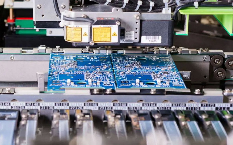
2. Component Placement: Pick-and-place machines accurately position components on the board[6].
3. Reflow Soldering: The PCB passes through a reflow oven, melting the solder paste and forming solder joints[8].
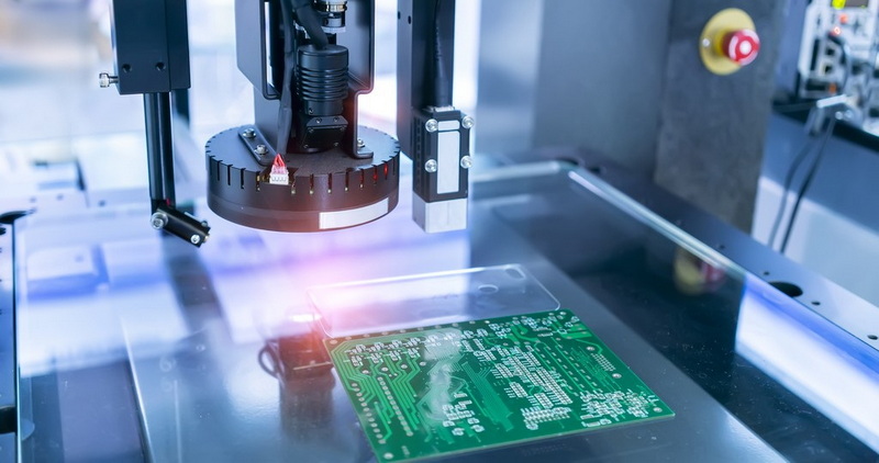
4. Inspection and Testing: Automated optical inspection (AOI) and electrical testing ensure quality.
Best Practices for SMT PCB Design
To optimize your PCB design for SMT assembly:
- Use consistent component orientations to simplify assembly
- Avoid placing components too close to board edges
- Design for panelization if producing in volume
- Include tooling holes and fiducial marks for accurate assembly
- Consider using no-clean flux to eliminate the need for post-assembly cleaning
Common Challenges in SMT PCB Design
Designing PCBs for SMT assembly can present several challenges:
- Component density limitations
- Thermal management in compact designs
- Signal integrity issues in high-speed circuits
- Balancing cost and performance in component selection
Addressing these challenges often requires a combination of careful planning, simulation, and prototyping.
Future Trends in SMT PCB Design
As technology advances, SMT PCB design continues to evolve. Some emerging trends include:
- Increased use of 3D component packages
- Integration of embedded components within PCB layers
- Advanced materials for improved thermal and electrical performance
- AI-assisted PCB design and optimization
Staying informed about these trends can help you design more advanced and competitive products.
Conclusion
Designing a PCB for SMT assembly requires careful consideration of numerous factors, from component selection to layout optimization and manufacturability. By following the guidelines and best practices outlined in this article, you can create PCB designs that are not only functional but also optimized for efficient and reliable SMT assembly. Remember that successful PCB design is often an iterative process, and collaboration with your PCB manufacturer and assembly house can lead to improved outcomes.

FAQ
1. What are the main advantages of SMT over through-hole technology?
SMT offers several advantages over through-hole technology:
- Smaller component sizes, allowing for more compact designs
- Faster assembly process, reducing manufacturing time and costs
- Improved electrical performance due to shorter lead lengths
- Better mechanical performance under shock and vibration
- Potential for double-sided component placement
2. How do I choose the right solder paste for my SMT PCB?
Selecting the appropriate solder paste involves considering:
- The alloy composition (lead-free vs. leaded)
- Melting temperature range
- Particle size (finer for smaller components)
- Flux type (no-clean, water-soluble, or rosin-based)
- Viscosity and printability
- Compatibility with your reflow profile and component requirements
3. What are some common SMT component package types?
Common SMT package types include:
- Chip components (resistors, capacitors)
- SOT (Small Outline Transistor)
- SOIC (Small Outline Integrated Circuit)
- QFP (Quad Flat Package)
- BGA (Ball Grid Array)
- QFN (Quad Flat No-lead)
- LGA (Land Grid Array)
4. How can I improve the thermal management of my SMT PCB design?
To enhance thermal management in SMT PCB designs:
- Use thermal vias to conduct heat away from components
- Implement copper pours and heat sinks for high-power components
- Consider using thermal interface materials
- Optimize component placement for better heat distribution
- Use PCB materials with higher thermal conductivity for critical areas
5. What are some common SMT assembly defects and how can I prevent them in my design?
Common SMT assembly defects include:
- Solder bridges: Prevent by proper pad design and solder paste application
- Tombstoning: Avoid by balanced pad design and proper component placement
- Component misalignment: Use fiducial marks and proper pick-and-place programming
- Insufficient solder: Ensure proper pad sizes and solder paste volume
- Solder voids: Use appropriate solder paste and optimize reflow profile
Citations:
[1] https://jlcpcb.com/blog/design-process-of-a-surface-mount-pcb
[2] https://insightsolutionsglobal.com/smt-surface-mount-technology-manufacturing-process/
[3] https://patents.google.com/patent/CN112040669B/zh
[4] https://www.pcbelec.com/pcb-assembly/smt-pcb-assembly
[5] https://www.youtube.com/watch?v=T2SK30JRs_E
[6] https://blogs.sw.siemens.com/valor-dfm-solutions/how-to-optimize-pcb-design-for-the-smt-assembly-process-flow/
[7] https://www.viasion.com/blog/what-are-the-steps-in-smt-assembly-process/
[8] https://www.ablcircuits.co.uk/blog/what-is-the-smt-process-and-why-should-oems-care/


