Content Menu
● Introduction
● The History of Surface Mount Technology
>> Early Developments
>> The 1970s and 1980s: The Rise of SMT
>> The 1990s and Beyond: Widespread Adoption
● Advantages of Surface Mount Technology
>> Increased Component Density
>> Enhanced Performance
>> Cost Efficiency
>> Improved Reliability
● The SMT Manufacturing Process
>> Design and Layout
>> Printing the Solder Paste
>> Component Placement
>> Reflow Soldering
>> Inspection and Testing
● Challenges and Considerations
>> Component Size and Handling
>> Thermal Management
>> Design Complexity
● The Future of Surface Mount Technology
>> Continued Innovation
>> The Role of 3D Printing
>> Sustainability Considerations
● Conclusion
● Related Questions
>> 1. What is the difference between surface mount technology and through-hole technology?
>> 2. What are the main advantages of using SMT in PCB manufacturing?
>> 3. How does the SMT manufacturing process work?
>> 4. What challenges are associated with surface mount technology?
>> 5. What is the future of surface mount technology?
Introduction
Surface Mount Technology (SMT) has fundamentally transformed the landscape of printed circuit board (PCB) manufacturing. This innovative method allows electronic components to be mounted directly onto the surface of PCBs, eliminating the need for traditional through-hole mounting techniques. The evolution of SMT has led to significant advancements in the efficiency, size, and reliability of electronic devices. This article explores the history of surface mount technology, its impact on PCB manufacturing, and the reasons behind its widespread adoption in the electronics industry.

The History of Surface Mount Technology
Early Developments
The origins of surface mount technology can be traced back to the 1960s when the need for smaller and more efficient electronic devices began to emerge. Early SMT concepts were developed to address the limitations of through-hole technology, which required components to be inserted into holes drilled into the PCB. This method was not only time-consuming but also limited the density of components that could be placed on a board.
The 1970s and 1980s: The Rise of SMT
By the 1970s, advancements in materials and manufacturing processes paved the way for the practical implementation of SMT. The introduction of automated assembly techniques, such as pick-and-place machines, allowed for faster and more accurate placement of components. During this period, SMT gained traction in the industry, particularly in the production of consumer electronics, telecommunications equipment, and computers.
The 1990s and Beyond: Widespread Adoption
The 1990s marked a significant turning point for SMT as it became the dominant method for PCB assembly. The miniaturization of electronic components, coupled with the increasing demand for compact devices, further fueled the adoption of SMT. Manufacturers began to recognize the benefits of SMT, including reduced assembly time, lower production costs, and improved performance of electronic devices.
Advantages of Surface Mount Technology
Increased Component Density
One of the most significant advantages of SMT is its ability to accommodate a higher density of components on a PCB. By mounting components directly onto the surface, manufacturers can utilize both sides of the board, maximizing space and allowing for more complex circuit designs. This increased density is particularly beneficial in the production of compact devices such as smartphones, tablets, and wearables.
Enhanced Performance
SMT components are typically smaller and lighter than their through-hole counterparts, which contributes to the overall performance of electronic devices. The reduced size of SMT components allows for shorter electrical paths, minimizing signal loss and improving the speed of data transmission. Additionally, the lower weight of SMT components can lead to lighter and more portable devices.
Cost Efficiency
The automation of SMT assembly processes has led to significant cost savings for manufacturers. Automated pick-and-place machines can quickly and accurately place components on PCBs, reducing labor costs and increasing production speed. Furthermore, the ability to use smaller components can lead to lower material costs, making SMT a more economical choice for manufacturers.
Improved Reliability
SMT has been shown to enhance the reliability of electronic devices. The soldering process used in SMT creates a strong bond between the component and the PCB, reducing the risk of mechanical failure. Additionally, the absence of leads that extend through the board minimizes the potential for solder joint fatigue, which can occur in through-hole components.
The SMT Manufacturing Process
Design and Layout
The first step in the SMT manufacturing process involves designing the PCB layout. Engineers use specialized software to create a design that optimizes the placement of components while considering factors such as signal integrity and thermal management. The layout must accommodate the specific dimensions and characteristics of the SMT components being used.

Printing the Solder Paste
Once the design is finalized, solder paste is applied to the PCB using a stencil. The solder paste consists of tiny solder balls suspended in a flux medium, which helps to ensure a strong bond between the components and the board. Accurate application of solder paste is crucial, as it determines the quality of the solder joints.
Component Placement
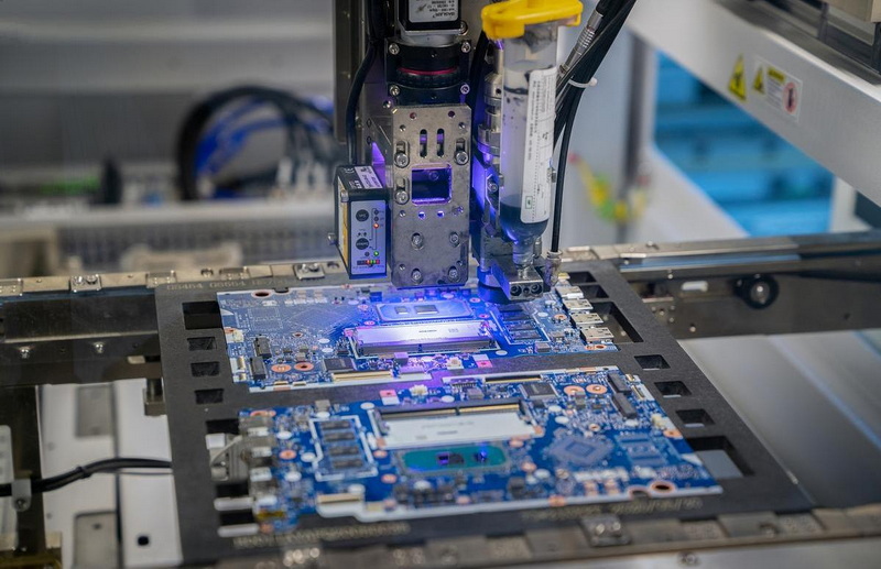
After the solder paste is applied, automated pick-and-place machines are used to position the SMT components onto the PCB. These machines are equipped with advanced vision systems that ensure precise placement, reducing the risk of errors. The placement process is rapid, allowing for high-volume production.
Reflow Soldering
Once the components are placed, the PCB undergoes a reflow soldering process. The board is heated in a controlled environment, causing the solder paste to melt and form a solid connection between the components and the PCB. This process is critical for ensuring the reliability of the solder joints.
Inspection and Testing
After soldering, the PCBs are inspected for defects using automated optical inspection (AOI) systems. These systems can quickly identify issues such as misaligned components or insufficient solder joints. Additionally, functional testing is performed to ensure that the assembled PCBs meet the required specifications.
Challenges and Considerations
Component Size and Handling
While SMT offers many advantages, it also presents challenges related to the handling of small components. The tiny size of SMT devices can make them difficult to manipulate, requiring specialized equipment and techniques for assembly. Manufacturers must invest in training and technology to ensure proper handling and placement.
Thermal Management
The increased density of components on SMT boards can lead to thermal management challenges. As more components are packed into a smaller space, the risk of overheating increases. Manufacturers must implement effective thermal management strategies, such as heat sinks and thermal vias, to dissipate heat and maintain optimal operating temperatures.
Design Complexity
The design of SMT PCBs can be more complex than traditional through-hole designs. Engineers must consider factors such as component placement, signal integrity, and thermal management during the design process. This complexity can lead to longer design cycles and increased costs if not managed effectively.
The Future of Surface Mount Technology
Continued Innovation
As technology continues to evolve, so too will surface mount technology. Innovations in materials, manufacturing processes, and design software are expected to drive further advancements in SMT. For example, the integration of artificial intelligence and machine learning into the manufacturing process could enhance efficiency and reduce errors.
The Role of 3D Printing
3D printing is emerging as a complementary technology to SMT, offering new possibilities for PCB manufacturing. The ability to create complex geometries and integrate components directly into the PCB could revolutionize the way electronic devices are designed and assembled.
Sustainability Considerations
As the electronics industry faces increasing pressure to adopt sustainable practices, SMT will play a crucial role in reducing waste and improving energy efficiency. The smaller size of SMT components can lead to less material waste, and advancements in recycling technologies will further enhance the sustainability of PCB manufacturing.
Conclusion
Surface Mount Technology has revolutionized PCB manufacturing by enabling the production of smaller, lighter, and more reliable electronic devices. Its history reflects a continuous evolution driven by the need for efficiency and performance in the electronics industry. As SMT continues to advance, it will undoubtedly play a pivotal role in shaping the future of electronic manufacturing.

Related Questions
1. What is the difference between surface mount technology and through-hole technology?
Surface mount technology (SMT) involves mounting components directly onto the surface of a PCB, while through-hole technology requires components to be inserted into holes drilled into the board. SMT allows for higher component density and is generally more efficient.
2. What are the main advantages of using SMT in PCB manufacturing?
The main advantages of SMT include increased component density, enhanced performance, cost efficiency, and improved reliability of electronic devices.
3. How does the SMT manufacturing process work?
The SMT manufacturing process involves designing the PCB layout, applying solder paste, placing components, reflow soldering, and inspecting the final product for defects.
4. What challenges are associated with surface mount technology?
Challenges include handling small components, managing thermal issues due to increased density, and the complexity of PCB design.
5. What is the future of surface mount technology?
The future of SMT includes continued innovation, the integration of 3D printing, and a focus on sustainability in electronic manufacturing.


