Content Menu
● Understanding the SMT Assembly Process
● Design Phase Considerations
>> PCB Size and Thickness
>> Component Selection and Placement
>> Via Design
● Design for Manufacturability (DFM) Principles
● Fiducial Marks and Tooling Strips
>> Fiducial Marks
>> Tooling Strips
● Solder Pad Design
● Component Spacing Guidelines
● Automated Component Placement Optimization
● Test Point Integration
● Material Selection
● Design Software and Analysis Tools
● Collaboration Between Design and Manufacturing Teams
● Conclusion
● FAQ
>> 1. What are the key benefits of optimizing PCB design for SMT assembly?
>> 2. How does component spacing affect SMT assembly?
>> 3. What role do fiducial marks play in SMT assembly?
>> 4. How can AI and machine learning improve SMT assembly processes?
>> 5. What are the most common mistakes in PCB design that affect SMT assembly?
● Citations:
In the ever-evolving world of electronics manufacturing, optimizing PCB (Printed Circuit Board) design for efficient SMT (Surface Mount Technology) assembly is crucial for producing high-quality, cost-effective electronic products. This article will explore various strategies and guidelines to enhance PCB design for seamless SMT assembly, ultimately improving production efficiency and product reliability.

Understanding the SMT Assembly Process
Before delving into optimization techniques, it's essential to understand the SMT assembly process. SMT involves placing surface mount components directly onto the PCB surface, as opposed to through-hole technology[3]. The process typically includes the following steps:
1. Applying solder paste using stencils
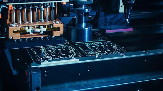
2. Picking and placing components
3. Optical inspection
4. Reflow soldering
5. Final inspection
Understanding this process is crucial for designers to make informed decisions that will streamline the assembly workflow.
Design Phase Considerations
PCB Size and Thickness
The design phase is critical in optimizing PCB for SMT assembly. One of the primary considerations is the PCB size and thickness. The design size must meet the maximum and minimum size requirements of the printer and chip mounter, typically ranging from 50mm x 50mm to 330mm x 250mm (or 410mm x 360mm)[2]. If the PCB is too thin, its design size should not be too large to prevent deformation due to reflow temperature. The ideal length-to-width ratio is 4:3 or 3:2[2].
Component Selection and Placement
Careful selection and placement of components are vital for efficient SMT assembly. Designers should aim to reduce the number of components where possible, as unnecessary clutter can compromise PCB quality and increase assembly costs[4]. When placing components, consider the following guidelines:
- Align SMT components in a single direction, especially for components with pin 1 designation[10]
- Ensure adequate spacing between components to facilitate soldering and prevent shorts
- Consider the lead length of SMT components to provide sufficient exposed points for solder joints[4]
Via Design
Proper via design is crucial for efficient signal transmission through the circuit board. Consider the following factors:
- Optimize via diameter for adequate current flow
- Ensure proper aspect ratio for effective layer connection
- Place vias near the components they are connecting
- Space vias apart to prevent short circuits and optimize board space[2]
Design for Manufacturability (DFM) Principles
Implementing Design for Manufacturability (DFM) principles is essential for optimizing PCB design for SMT assembly. DFM focuses on creating PCB layouts that are conducive to efficient assembly processes[1]. By following DFM guidelines, designers can:
- Reduce complex component placement
- Minimize the need for manual intervention
- Improve assembly speed
- Reduce the risk of errors
- Ensure product longevity and reliability[1]
Fiducial Marks and Tooling Strips
Fiducial Marks
Fiducial marks are crucial for accurate component placement, especially for QFP or BGA type components. These marks, located at the corners of a PCB or component, help the optical system pinpoint component coordinates with high accuracy[10]. Always include fiducial markers at the corners of the PCB to ensure precise assembly.
Tooling Strips
Tooling strips are equally important, particularly when space on the PCB is limited. Create tooling strips of at least 6 mm to allow machines ample grip during assembly. Adding V-scores on the strips makes it easy to remove them later in the process[10].
Solder Pad Design
Proper solder pad design is crucial for successful SMT assembly. There are two types of land patterns used for surface-mount devices:
1. Solder mask-defined (SMD) pads
2. Non-solder mask-defined (NSMD) pads
NSMD pads are generally recommended as they provide a larger metal area for solder to anchor to the edges of the metal pads, improving solder joint reliability[5]. It's important to use only one type of pad (NSMD or SMD) and one type of pad surface finish at a given footprint[5].
Component Spacing Guidelines
Ensuring adequate spacing between SMD components is crucial for successful solder pasting and preventing solder joint issues. Consider the following spacing guidelines:
- Homogeneous SMD components: ≥0.3mm
- Heterogeneous SMD components: ≥0.13*H+0.3mm (where H is the maximum height difference of neighboring components)[9]

Automated Component Placement Optimization
Leveraging advanced technologies like AI and machine learning can significantly optimize the SMT assembly process. For instance, reinforcement learning models can be used to determine the most efficient sequence for mounting electronic components on PCBs, reducing overall process time[7].
These AI-driven approaches can:
- Analyze PCB layouts to determine optimal component placement sequences
- Minimize overall cycle time in the assembly process
- Adapt to different machines and manufacturing setups[7]
Test Point Integration
Incorporating test points in your PCB design is crucial for easy testing and troubleshooting after assembly. When adding test points:
- Locate them in easily accessible areas
- Clearly mark test points to facilitate testing
- Use test points to measure signals at different points on the board[3]
Material Selection
The choice of PCB material can significantly impact the SMT assembly process and the final product's performance. Consider factors such as:
- Thermal stability during reflow soldering
- Coefficient of thermal expansion (CTE)
- Dielectric properties
- Moisture absorption
Selecting the right material can improve the reliability of solder joints and overall PCB performance.
Design Software and Analysis Tools
Utilizing the right PCB design and analysis software is crucial for optimizing designs for SMT assembly. Advanced tools like Cadence Allegro allow designers to set assembly rules and prevent missing essential SMT assembly optimizations[10]. These software solutions can help:
- Implement DFM guidelines
- Analyze component placement and spacing
- Simulate thermal profiles during reflow soldering
- Identify potential issues before production
Collaboration Between Design and Manufacturing Teams
Effective collaboration between design and manufacturing teams is essential for successful SMT assembly optimization. This collaboration ensures that:
- Design decisions align with manufacturing capabilities
- Potential issues are identified and addressed early in the design process
- Manufacturing feedback is incorporated into future designs
- The overall production process is streamlined and efficient[1]
Conclusion
Optimizing PCB design for efficient SMT assembly is a multifaceted process that requires careful consideration of various factors. From the initial design phase to component selection, placement, and manufacturing considerations, each step plays a crucial role in ensuring a smooth and efficient assembly process.
By following PCB design and SMT assembly guidelines, implementing DFM principles, leveraging advanced technologies, and fostering collaboration between design and manufacturing teams, designers can create PCBs that are not only functionally superior but also optimized for efficient production.
As technology continues to evolve, staying updated with the latest PCB design and SMT assembly guidelines will be crucial for maintaining a competitive edge in the electronics manufacturing industry. By continually refining and optimizing PCB designs for SMT assembly, manufacturers can achieve higher production efficiency, reduced costs, and improved product quality.

FAQ
1. What are the key benefits of optimizing PCB design for SMT assembly?
Optimizing PCB design for SMT assembly offers several benefits, including:
- Improved production efficiency
- Reduced manufacturing costs
- Enhanced product reliability
- Faster time-to-market
- Fewer assembly errors and rework requirements
2. How does component spacing affect SMT assembly?
Proper component spacing is crucial for successful SMT assembly because:
- It allows for efficient solder paste application
- It prevents solder bridging between components
- It facilitates easier inspection and rework if needed
- It ensures proper heat distribution during reflow soldering
3. What role do fiducial marks play in SMT assembly?
Fiducial marks are essential in SMT assembly for the following reasons:
- They provide reference points for accurate component placement
- They help optical systems align PCBs correctly
- They improve the precision of pick-and-place machines
- They are particularly crucial for placing fine-pitch components like BGAs and QFPs
4. How can AI and machine learning improve SMT assembly processes?
AI and machine learning can enhance SMT assembly in several ways:
- Optimizing component placement sequences
- Reducing overall assembly cycle time
- Predicting and preventing potential defects
- Adapting to different PCB designs and manufacturing setups
- Continuously improving processes through data analysis
5. What are the most common mistakes in PCB design that affect SMT assembly?
Common PCB design mistakes that impact SMT assembly include:
- Insufficient component spacing
- Improper pad design
- Lack of fiducial marks
- Incorrect component orientation
- Inadequate consideration of thermal management
- Failure to implement DFM principles
Citations:
[1] https://www.thinksemiinfotech.com/pcb-assembly/pcb-smt-assembly-process-helping-you-reduce-production-costs/
[2] https://www.myemssolutions.com/6-considerations-for-smt-pcb-design/
[3] https://blogs.sw.siemens.com/valor-dfm-solutions/how-to-optimize-pcb-design-for-the-smt-assembly-process-flow/
[4] https://www.hayawin.com/resources/how-to-optimize-pcb-design-for-smt-assembly-process-flow.html
[5] https://www.analog.com/en/resources/design-notes/smt-assembly-and-pcb-design-guidelines-for-leaded-packages.html
[6] https://baike.baidu.com/item/%E7%94%B5%E5%AD%90%E7%BB%84%E8%A3%85%E6%8A%80%E6%9C%AF%E4%B8%93%E4%B8%9A%E8%8B%B1%E8%AF%AD/12086345
[7] https://www.makinarocks.ai/en/use-case/smt-optimization-for-pcb/
[8] https://www.viasion.com/blog/ultimate-guide-to-pcb-smt-assembly-process/
[9] https://wellerpcb.com/pcb-layout-guidelines-for-smt-assembly-process-limits
[10] https://resources.pcb.cadence.com/blog/2020-how-to-optimize-pcb-design-for-smt-assembly-process-flow


