Content Menu
● Introduction to SMT Assembly
>> Benefits of SMT Assembly
● SMT PCB Design Guidelines
>> 1. Use Proper Footprints
>> 2. Component Placement
>> 3. Avoid Overcrowding
>> 4. Follow Design for Manufacturing (DFM) Guidelines
>> 5. Consider Rework and Repairability
● Best Practices for SMT PCB Design
>> Plan for Assembly Early
>> Use Design for Manufacturability (DFM) Guidelines
>> Optimize for SMT Assembly
● Tools and Techniques for Efficient SMT Assembly
>> Stencils and Solder Paste Application
>> DIY SMT Assembly
>> Automated Assembly Systems
● Challenges and Considerations
>> Component Selection
>> Thermal Management
>> Mixing Technologies
>> Environmental Considerations
● Advanced Techniques in SMT Assembly
>> High-Density Interconnects (HDI)
>> Flexible PCBs
>> 3D Printing and Additive Manufacturing
● Conclusion
● Frequently Asked Questions
>> 1. What are the benefits of using SMT assembly over through-hole assembly?
>> 2. How important is component orientation in SMT assembly?
>> 3. What are the key considerations for spacing between SMT components?
>> 4. Why is following DFM guidelines important in PCB design?
>> 5. How can panelization improve SMT assembly efficiency?
Optimizing a PCB (Printed Circuit Board) layout for SMT (Surface Mount Technology) assembly efficiency is crucial for ensuring that electronic devices are manufactured quickly, reliably, and cost-effectively. SMT assembly involves mounting components directly onto the surface of the PCB, which is faster and more precise than traditional through-hole assembly. However, it requires careful design optimization to avoid assembly errors and ensure high manufacturing yields. In this article, we will explore the key guidelines and strategies for optimizing PCB layouts for SMT assembly efficiency.

Introduction to SMT Assembly
SMT assembly is a widely used technique in modern electronics manufacturing due to its efficiency and cost-effectiveness. It involves using automated machines to place components onto the PCB, which significantly reduces assembly time and increases precision compared to manual through-hole assembly methods. However, successful SMT assembly depends heavily on the quality of the PCB design.
Benefits of SMT Assembly
- Speed and Efficiency: SMT assembly is much faster than through-hole assembly, allowing for higher production volumes in less time.
- Cost-Effectiveness: By reducing labor and material costs, SMT assembly is more economical for large-scale production.
- Precision: Automated machines ensure accurate component placement, minimizing errors.
SMT PCB Design Guidelines
To optimize a PCB layout for SMT assembly, designers must adhere to specific guidelines that ensure efficient and reliable manufacturing. Here are some key considerations:
1. Use Proper Footprints
Using accurate and manufacturer-specified component footprints is essential for SMT assembly. These footprints define the size, shape, and location of components on the board, ensuring proper alignment and placement during assembly. Following IPC (Institute for Printed Circuits) specifications helps maintain the correct toe, heel, side, and periphery distances during soldering.
2. Component Placement
- Keep SMT Components on One Side: Ideally, placing all SMT components on one side of the board simplifies the assembly process, increases yield, and reduces costs. However, with the trend towards miniaturization, using both sides is common but increases assembly complexity.
- Uniform Orientation: Ensure all components are oriented in the same direction to facilitate faster and more accurate assembly. Mixed orientations can lead to assembly errors during inspection.
3. Avoid Overcrowding
Maintaining adequate spacing between components is crucial. Too little space can complicate solder paste application and increase the risk of solder bridges between pads. Recommended spacings include:
- Homogeneous Components: ≥0.3 mm
- Heterogeneous Components: ≥0.13*H + 0.3 mm, where H is the maximum height difference between neighboring components.
4. Follow Design for Manufacturing (DFM) Guidelines
DFM guidelines, typically provided by the PCB manufacturer, offer critical advice on component placement, orientation, and spacing. Adhering to these guidelines improves manufacturing yield and reduces defects.
5. Consider Rework and Repairability
Designing for easy rework and repair can save time and costs in the long run. Avoid placing components under other components, as this complicates inspection and repair.

Best Practices for SMT PCB Design
Plan for Assembly Early
- Early Planning: Consider assembly requirements from the conceptual stage to prevent costly redesigns and ensure efficient assembly processes.
- Standardized Components: Use standardized components and ensure correct orientation to avoid assembly errors.
Use Design for Manufacturability (DFM) Guidelines
Consult DFM guidelines for recommendations on component spacing, solder pad sizes, and other critical design elements. These guidelines help improve manufacturing yield and reduce defects.
Optimize for SMT Assembly
- SMT-Specific Components: Choose components suitable for SMT assembly and ensure solder pads are designed accordingly.
- Panelization: Consider panelizing PCBs to optimize material use and improve assembly efficiency.
Tools and Techniques for Efficient SMT Assembly
Stencils and Solder Paste Application
Using stencils for solder paste application is crucial for efficient SMT assembly. This method ensures accurate paste placement, which is essential for reliable solder joints. Solder paste inspection (SPI) tools analyze paste volume and location to ensure quality.
DIY SMT Assembly
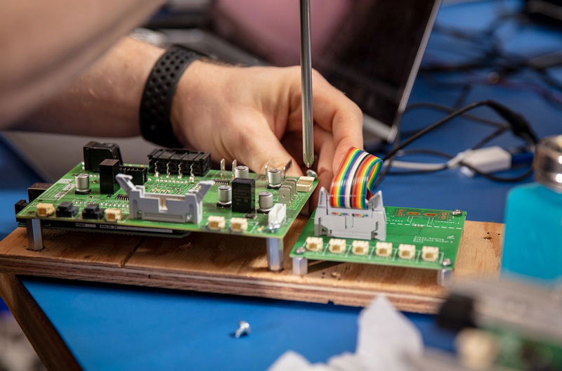
For small-scale or prototype assembly, using a stencil with a soldering station can achieve production-quality results. Tools like curved tweezers facilitate component placement, especially in high-density areas.
Automated Assembly Systems
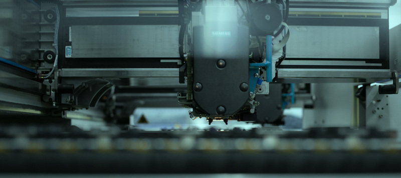
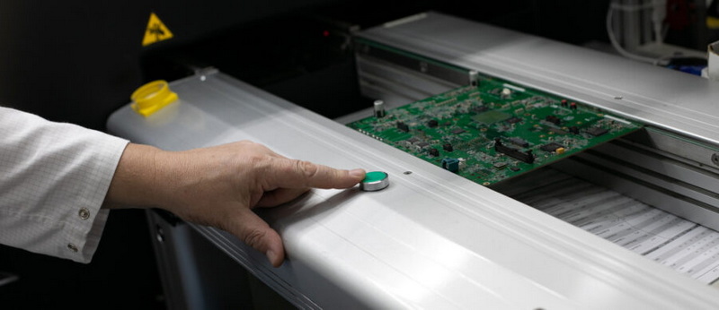
Investing in automated assembly systems can significantly enhance production efficiency. These systems include pick-and-place machines, reflow ovens, and inspection tools that ensure high-quality assembly.
Challenges and Considerations
Component Selection
Choosing the right package size is important. Larger components can simplify assembly if space allows, while smaller components like 0201 resistors may require more precise handling.
Thermal Management
Distribute large components evenly to achieve optimal thermal distribution during solder reflow. This helps prevent overheating and ensures consistent soldering quality.
Mixing Technologies
Avoid mixing SMT and through-hole technologies unless necessary, as this can complicate the assembly process and increase costs.
Environmental Considerations
Ensure that PCB materials and components comply with environmental regulations such as RoHS (Restriction of Hazardous Substances) to avoid compliance issues.
Advanced Techniques in SMT Assembly
High-Density Interconnects (HDI)
HDI PCBs allow for more complex designs with higher component densities. They require precise design and assembly techniques to ensure reliability.
Flexible PCBs
Flexible PCBs offer flexibility in design and can be used in applications where traditional rigid PCBs are not suitable. However, they require specialized assembly techniques.
3D Printing and Additive Manufacturing
Emerging technologies like 3D printing can create complex geometries and structures that traditional PCB manufacturing cannot achieve. However, integrating these technologies into SMT assembly is still in its early stages.
Conclusion
Optimizing a PCB layout for SMT assembly efficiency involves careful planning, adherence to design guidelines, and consideration of manufacturing constraints. By following these strategies, designers can improve production efficiency, reduce costs, and enhance the reliability and performance of electronic devices.

Frequently Asked Questions
1. What are the benefits of using SMT assembly over through-hole assembly?
SMT assembly offers several benefits, including faster production times, lower costs, and higher precision. It is more suitable for large-scale manufacturing due to its efficiency and cost-effectiveness.
2. How important is component orientation in SMT assembly?
Component orientation is crucial in SMT assembly. Uniform orientation ensures faster and more accurate assembly, reducing errors during the inspection process.
3. What are the key considerations for spacing between SMT components?
Maintaining adequate spacing between components is essential to avoid solder bridges and ensure easy solder paste application. Recommended spacings vary based on component types and heights.
4. Why is following DFM guidelines important in PCB design?
Following DFM guidelines is important because they provide critical advice on component placement, orientation, and spacing, which can significantly improve manufacturing yield and reduce defects.
5. How can panelization improve SMT assembly efficiency?
Panelization optimizes material use and improves assembly efficiency by allowing multiple PCBs to be assembled simultaneously, which can reduce manufacturing costs and enhance production speed.


