Content Menu
● Understanding SMT Solder Paste and Stencils
● Key Factors for Accurate Solder Paste Deposition
>> 1. Stencil Design and Engineering
>> 2. Proper Stencil Alignment and Setup
>> 3. Controlled Solder Paste Application
>> 4. Stencil Cleaning and Maintenance
>> 5. Use of Solder Paste Inspection (SPI) Tools
● Step-by-Step Process for Accurate Solder Paste Deposition Using Stencils
>> 1. Preparation:
>> 2. Stencil and PCB Alignment:
>> 3. Solder Paste Application:
>> 4. Stencil Removal:
>> 5. Inspection:
>> 6. Component Placement and Reflow:
>> 7. Stencil Cleaning:
● Challenges and Solutions in SMT Stencil Engineering
>> Fine-Pitch Components and Miniaturization
>> Complex PCB Layouts with Mixed Components
>> Solder Paste Viscosity and Storage Issues
>> Stencil Wear and Maintenance
● Advanced Techniques and Innovations in SMT Solder Paste Stencil Engineering
>> Laser-Cut Apertures with Micro-Texturing
>> Step Stencils and Area Array Stencils
>> Automated Stencil Inspection Systems
>> Integration with Industry 4.0 and Data Analytics
● Conclusion
● FAQ
>> 1. What is the role of a stencil in SMT solder paste application?
>> 2. How do engineers determine the right stencil thickness?
>> 3. Why is stencil cleaning important?
>> 4. How do solder paste inspection (SPI) tools improve accuracy?
>> 5. What are common challenges in stencil engineering for complex PCBs?
In the surface mount technology (SMT) assembly process, the accurate deposition of solder paste is critical for achieving reliable electrical connections and high-quality printed circuit board (PCB) assemblies. Engineers rely heavily on SMT solder paste stencils to precisely apply solder paste onto PCB pads before component placement and reflow soldering. This article explores the best practices, engineering considerations, and techniques that SMT engineers use to ensure accurate solder paste deposits using stencils.

Understanding SMT Solder Paste and Stencils
Solder paste is a viscous mixture of powdered metal solder and flux medium, designed to temporarily hold surface mount components on PCB pads before melting and forming permanent joints during reflow soldering. The stencil, typically made from stainless steel or other metals, acts as a mask with apertures that correspond exactly to the PCB pad layout. When solder paste is applied over the stencil, it passes through these apertures and deposits precisely on the PCB pads underneath.
The stencil's role is fundamental in the SMT process, as it governs the volume, shape, and location of solder paste deposits. Any variation or misalignment can cause defects such as insufficient solder, bridging, or tombstoning, which affect the yield and reliability of the final product.
Key Factors for Accurate Solder Paste Deposition
1. Stencil Design and Engineering
The first step to ensuring accurate solder paste deposits begins with the stencil design. SMT engineers must carefully engineer the stencil apertures to match the PCB pad geometry and component requirements. This involves:
- Aperture size and shape optimization: Apertures must be sized to deposit the correct volume of solder paste. Engineers calculate release ratios (aperture opening area to stencil thickness) to optimize paste release and avoid defects. For example, a release ratio of 0.66 or higher is generally recommended to ensure clean paste release.
- Stencil thickness selection: Thicker stencils deposit more solder paste volume, suitable for larger pads or components, while thinner stencils are used for fine-pitch devices to avoid excessive paste. Typical stencil thickness ranges from 75 to 150 microns, but fine-pitch components often require thinner stencils around 100 microns or less.
- Material and manufacturing precision: High-quality stainless steel stencils with precise laser-cut apertures provide better repeatability and durability than cheaper Mylar or foil stencils. Laser cutting ensures smooth aperture walls and consistent dimensions, which are critical for uniform paste deposition.
Experienced SMT engineers often handcraft aperture sizes or use advanced CAM tools with automation features to refine stencil designs, balancing speed and accuracy in new product introductions. Additionally, engineers may use specialized aperture shapes such as trapezoidal or elliptical openings to improve paste release on challenging pad geometries.
2. Proper Stencil Alignment and Setup
Accurate alignment of the stencil to the PCB is crucial. Engineers use fiducial marks on both the PCB and stencil to align them precisely so that the stencil apertures match the PCB pads exactly. Misalignment can cause solder paste to be deposited off-pad, leading to soldering defects such as bridging or insufficient solder joints.
During setup, the stencil must be securely fixed to prevent movement during printing. Some engineers tape two sides of the stencil frame to allow slight flexibility while preventing rotation, especially when using flexible Mylar stencils. In automated SMT lines, precision stencil printers use vacuum and mechanical clamps to hold the stencil and PCB firmly, ensuring repeatable alignment with micron-level accuracy.
3. Controlled Solder Paste Application
The application technique affects the quality of the solder paste deposit:
- Paste temperature: Solder paste should be brought to room temperature before use to improve spreadability and consistency. Cold paste tends to be stiffer and harder to print, while overheated paste can dry out or separate.
- Squeegee technique: A squeegee (usually made of stainless steel or polyurethane) is used to spread solder paste evenly across the stencil. Engineers make a single, smooth pass to avoid lifting the stencil or causing smearing. The squeegee angle, pressure, and speed are carefully controlled to optimize paste transfer.
- Paste volume control: Applying too much or too little paste can cause defects. Engineers monitor paste volume and consistency, adjusting the amount applied and the squeegee pressure accordingly. For example, excessive paste volume can cause bridging between fine-pitch pads, while insufficient paste leads to weak solder joints.
4. Stencil Cleaning and Maintenance
A clean stencil ensures consistent paste deposition. Residual solder paste clogging apertures can reduce paste volume or cause uneven deposits. Engineers clean stencils regularly using rubbing alcohol or specialized cleaning solutions, wiping both sides thoroughly. Automated stencil cleaning machines are often used in high-volume production to maintain stencil aperture integrity.
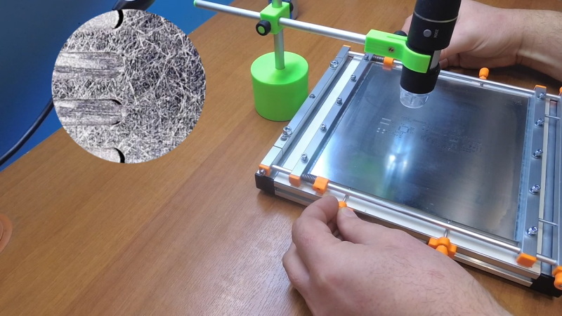
Regular inspection of stencil apertures for wear, deformation, or damage is essential. Over time, apertures can become enlarged or distorted, negatively impacting paste volume and print quality. Scheduled stencil replacement or refurbishment is part of good engineering practice.
5. Use of Solder Paste Inspection (SPI) Tools
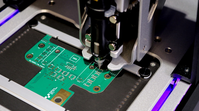
Modern SMT lines employ inline solder paste inspection (SPI) tools to measure solder paste deposits immediately after printing. These tools use high-resolution cameras and software algorithms to inspect paste volume, height, and area coverage for each pad.
Advancements in SPI technology have improved measurement accuracy, especially for low-volume deposits needed for fine-pitch components. Engineers rely on SPI feedback to adjust stencil design, printing parameters, and paste formulation to optimize deposition accuracy. SPI data can be integrated into statistical process control (SPC) systems to monitor trends and detect process drifts early.

Step-by-Step Process for Accurate Solder Paste Deposition Using Stencils
1. Preparation:
- Remove solder paste from refrigeration and allow it to warm to room temperature, typically for 2-4 hours.
- Inspect PCB for cleanliness and correct layout, ensuring no contamination or oxidation on pads.
- Verify stencil matches the PCB and check for any clogs, burrs, or damage.
2. Stencil and PCB Alignment:
- Align fiducial marks on stencil and PCB using manual or automated alignment tools.
- Secure stencil to PCB or printing frame to prevent movement during printing.
3. Solder Paste Application:
- Apply a controlled amount of solder paste at one edge of the stencil.
- Use a squeegee to spread paste evenly across stencil apertures with consistent pressure and speed.
4. Stencil Removal:
- Lift stencil carefully in one smooth motion to avoid smearing or lifting paste off pads.
5. Inspection:
- Use SPI tools or visual inspection to verify paste volume, height, and placement.
- Identify any defects such as insufficient paste, bridging, or smearing.
6. Component Placement and Reflow:
- Place components on paste deposits and proceed with reflow soldering, ensuring that paste volume and placement support reliable solder joints.
7. Stencil Cleaning:
- Clean stencil immediately after use to prevent paste drying and clogging.
- Inspect apertures and prepare stencil for the next printing cycle.
Challenges and Solutions in SMT Stencil Engineering
Fine-Pitch Components and Miniaturization
As electronic devices become smaller and more complex, SMT engineers face the challenge of printing solder paste for fine-pitch components with pitches as small as 0.3 mm or less. This requires stencils with very small apertures and thinner thicknesses to avoid excessive paste volume that can cause bridging.
Solutions:
- Use ultra-thin stainless steel stencils (50-75 microns).
- Employ advanced aperture shapes such as trapezoidal or micro-venting to improve paste release.
- Optimize squeegee parameters and printing speed to minimize paste smearing.
Complex PCB Layouts with Mixed Components
Modern PCBs often feature a mix of component sizes, from large connectors to tiny ICs, requiring varied solder paste volumes. Balancing paste volume across these diverse pads is challenging.
Solutions:
- Customize aperture sizes individually for each pad type.
- Use step stencils or stencil with variable thickness zones.
- Implement SPI feedback loops to fine-tune paste volume per pad.
Solder Paste Viscosity and Storage Issues
Solder paste viscosity changes over time due to solvent evaporation or temperature fluctuations, affecting printability and paste release.
Solutions:
- Store solder paste under recommended refrigeration conditions.
- Use paste within its shelf life.
- Regularly stir paste to maintain homogeneity.
- Adjust printing parameters based on paste condition.
Stencil Wear and Maintenance
Repeated use causes stencil apertures to wear or deform, impacting print quality.
Solutions:
- Schedule regular stencil inspections using microscopes or optical tools.
- Replace or refurbish stencils as needed.
- Use high-quality stencils with durable coatings to extend life.
Advanced Techniques and Innovations in SMT Solder Paste Stencil Engineering
Laser-Cut Apertures with Micro-Texturing
Recent advances in laser cutting allow micro-texturing of aperture walls to improve solder paste release and reduce paste sticking inside apertures. This results in cleaner prints and less clogging.
Step Stencils and Area Array Stencils
Step stencils feature varying thicknesses across the stencil to deposit different paste volumes on different pads without changing aperture sizes. Area array stencils are designed specifically for BGA or CSP components with dense pad arrays.
Automated Stencil Inspection Systems
Automated optical inspection (AOI) systems for stencils detect aperture defects, burrs, or contamination before printing, preventing defective prints and reducing downtime.
Integration with Industry 4.0 and Data Analytics
SMT lines increasingly integrate stencil printing data with manufacturing execution systems (MES) and use data analytics to predict stencil wear, paste quality trends, and optimize maintenance schedules.
Conclusion
Accurate solder paste deposition using SMT solder paste stencils is a complex but critical task that SMT engineers must master to ensure high-quality PCB assemblies. It requires a combination of precise stencil design, meticulous alignment, controlled paste application, regular cleaning, and real-time inspection. By leveraging advanced stencil engineering practices, modern inspection tools, and data-driven process controls, engineers can optimize solder paste printing to minimize defects and maximize production yield. Continuous innovation in stencil materials, aperture design, and inspection technology further enhances the capability to meet the demands of miniaturization and complex PCB assemblies in today's electronics manufacturing landscape.

FAQ
1. What is the role of a stencil in SMT solder paste application?
A stencil acts as a mask with apertures that match PCB pads, enabling precise deposition of solder paste onto the PCB during the SMT assembly process. It controls the volume and location of solder paste deposits, which is essential for forming reliable solder joints.
2. How do engineers determine the right stencil thickness?
Stencil thickness is selected based on the required solder paste volume for the components; thicker stencils deposit more paste, while thinner stencils are used for fine-pitch devices to avoid excess paste. Typical thickness ranges from 75 to 150 microns, but fine-pitch applications often require thinner stencils.
3. Why is stencil cleaning important?
Cleaning removes residual solder paste that can clog apertures, ensuring consistent paste volume and preventing defects such as insufficient solder or bridging in subsequent prints. Regular cleaning also extends stencil life and maintains print quality.
4. How do solder paste inspection (SPI) tools improve accuracy?
SPI tools use high-resolution imaging to measure paste volume, height, and placement immediately after printing, allowing engineers to detect and correct errors early in the process. This feedback helps optimize stencil design and printing parameters, reducing defects.
5. What are common challenges in stencil engineering for complex PCBs?
Challenges include managing multiple aperture sizes, maintaining precision for fine-pitch components, balancing paste volume across diverse pad geometries, and dealing with solder paste viscosity variations. These require careful stencil design, process control, and inspection.


