Content Menu
● What is SMT Stencil Electropolishing?
● How SMT Stencil Electropolishing Works
● Benefits of SMT Stencil Electropolishing
● How SMT Stencil Electropolishing Reduces Defects in PCB Assembly
● Case Studies and Industry Insights
● Additional Surface Treatments Complementing Electropolishing
● Best Practices for Implementing SMT Stencil Electropolishing
● Conclusion
● FAQ
>> 1. What is the primary purpose of SMT stencil electropolishing?
>> 2. How does electropolishing reduce defects in PCB assembly?
>> 3. Can electropolishing be applied to all types of SMT stencils?
>> 4. How does electropolishing compare to mechanical polishing?
>> 5. Are there additional treatments that enhance the benefits of electropolishing?
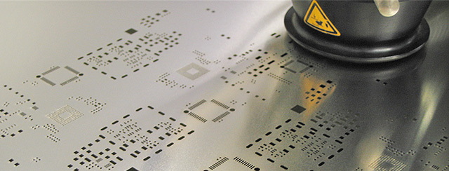
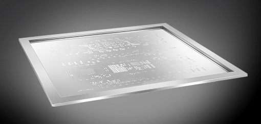
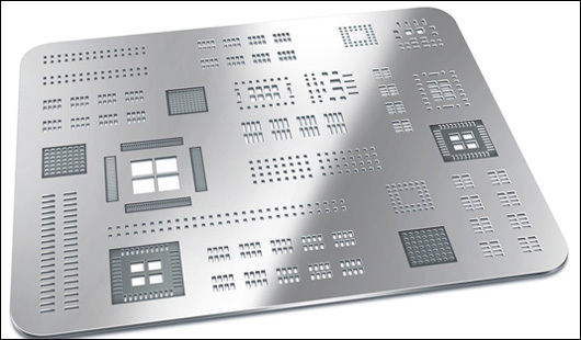
Surface Mount Technology (SMT) stencil electropolishing is an advanced finishing process applied to SMT stencils used in printed circuit board (PCB) assembly. This process has gained significant attention for its ability to enhance stencil quality and reduce defects during PCB assembly. This article explores the principles of SMT stencil electropolishing, its benefits, and its impact on defect reduction in PCB assembly.

What is SMT Stencil Electropolishing?
SMT stencil electropolishing, also known as electrolytic polishing or electrochemical deburring, is a process that smooths and levels the surface and aperture walls of SMT stencils by using an electrochemical reaction. During this process, the stencil acts as the anode and is immersed in an electrolyte solution. When a direct current is applied, microscopic protrusions on the stencil surface dissolve faster than the recessed areas due to uneven current density, resulting in a smoother and more uniform surface finish.
This process removes laser-induced micro-burrs and slag left on the aperture walls after laser cutting, which are common causes of solder paste printing defects. Electropolishing improves the cleanliness and flatness of the stencil surface without introducing additional stress or metamorphic layers, making it superior to mechanical polishing methods.
How SMT Stencil Electropolishing Works
The electropolishing process for SMT stencils involves several key steps:
1. Preparation: The laser-cut stencil is thoroughly cleaned to remove any contaminants and then fixed as the anode in an electropolishing tank filled with an electrolyte solution, typically a mixture of acids designed to dissolve metal ions selectively.
2. Electrochemical Reaction: A direct current is applied between the stencil (anode) and a cathode submerged in the electrolyte. The electric current causes metal ions on the stencil surface, especially on microscopic protrusions or burrs, to dissolve into the solution.
3. Surface Smoothing: Due to the higher current density on raised areas, these protrusions dissolve faster than recessed areas, resulting in a leveling effect. This smooths the microscopic roughness of the aperture walls and stencil surface.
4. Result: After a controlled period, the stencil surface becomes highly polished with reduced roughness and burrs, improving solder paste release and print quality.
This process is carefully controlled to avoid excessive material removal that could alter stencil aperture dimensions, which are critical for accurate solder paste deposition.
Benefits of SMT Stencil Electropolishing
The advantages of SMT stencil electropolishing are numerous and directly impact the quality and efficiency of PCB assembly:
- Improved Solder Paste Release: The smoother aperture walls reduce friction between the stencil and solder paste. This facilitates easier and more complete release of solder paste onto PCB pads, minimizing paste smearing and bridging defects.
- Reduced Defects: Burrs and rough edges left from laser cutting can trap solder paste or cause inconsistent paste deposits. Electropolishing removes these imperfections, reducing common SMT defects such as insufficient solder deposits, solder bridging between pads, and tombstoning of components.
- Enhanced Print Quality and Repeatability: Electropolishing can improve surface roughness by two levels on the Ra scale, resulting in more consistent solder paste deposits across multiple print cycles. This consistency is crucial for high-volume manufacturing and fine-pitch components.
- Stress-Free Surface Finish: Unlike mechanical polishing, which can introduce mechanical stress, deformation, or micro-cracks, electropolishing is a chemical process that leaves the stencil surface stress-free and maintains its structural integrity.
- Increased Durability: A smoother surface is less prone to solder paste buildup and easier to clean, extending the stencil's usable life and reducing downtime for maintenance.
- Efficiency and Scalability: Electropolishing is a fast process that can treat multiple stencils simultaneously, making it suitable for mass production environments without compromising quality.
- Compatibility with Complex Designs: Modern PCBs often require stencils with very fine apertures and complex geometries. Electropolishing is effective for thin-walled, complex-shaped stencils and very small aperture sizes, where mechanical polishing would be challenging or damaging.
How SMT Stencil Electropolishing Reduces Defects in PCB Assembly
Solder paste printing is a critical step in SMT assembly and is often the root cause of many defects. Defects such as insufficient solder, excessive solder, bridging, and misalignment can lead to poor electrical connections and rework or scrap.
Electropolished SMT stencils contribute to defect reduction in several ways:
- Consistent Paste Volume: The smoother aperture walls ensure that the solder paste volume deposited on each pad is consistent, reducing the risk of insufficient or excessive solder. This is especially important for fine-pitch components where small variations can cause failures.
- Better Paste Release: Reduced friction and burrs prevent solder paste from sticking inside the apertures, minimizing defects caused by incomplete paste transfer. This leads to cleaner prints and fewer solder bridging issues.
- Improved Alignment and Print Accuracy: Electropolishing helps maintain stencil flatness and aperture precision, which is crucial for accurate paste placement, especially for fine-pitch components and ball grid arrays (BGAs).
- Reduced Cavities and Voids: The smoother surface reduces microscopic cavities that can trap air or solder paste, improving solder joint reliability and reducing voids that can cause thermal and mechanical failures.
- Lower Tombstoning Rates: Tombstoning occurs when one end of a chip component lifts during reflow due to uneven solder paste deposits. Electropolished stencils help ensure even paste distribution, reducing this defect.
- Minimized Paste Smearing: Burrs and rough edges can cause solder paste to smear across pads during printing, leading to shorts and bridging. Electropolishing removes these burrs, resulting in cleaner paste application.

Case Studies and Industry Insights
Several industry reports and case studies highlight the benefits of SMT stencil electropolishing in real-world PCB assembly environments:
- A leading electronics manufacturer reported a 43% reduction in assembly defects after switching to electropolished stencils combined with optimized stencil design. Specific components saw defect reductions as high as 69%, demonstrating the significant impact on yield and quality.
- Another study showed that electropolishing improved solder paste print volume consistency by over 15%, which directly correlated with fewer rework cycles and higher first-pass yields.
- Electropolishing also contributed to extending stencil life by reducing solder paste buildup and easing cleaning processes, resulting in lower operational costs and less downtime.
Additional Surface Treatments Complementing Electropolishing
To further enhance stencil performance, some manufacturers combine electropolishing with additional surface treatments such as nano-coatings or nano-finishing. These treatments provide:
- Hydrophobic or Oleophobic Properties: Nano-coatings can repel solder paste, reducing adhesion and making stencil cleaning easier.
- Increased Durability: Protective coatings shield the stencil surface from corrosion and wear, extending operational life.
- Improved Paste Release: The combination of a smooth, electropolished surface with a nano-coating can significantly improve solder paste release, especially for challenging high-density or microelectronic assemblies.
- Reduced Cleaning Frequency: Enhanced surface properties reduce solder paste buildup, decreasing the need for frequent cleaning and improving production uptime.
Best Practices for Implementing SMT Stencil Electropolishing
To maximize the benefits of SMT stencil electropolishing, manufacturers should consider the following best practices:
- Stencil Material Selection: Stainless steel is the most common stencil material compatible with electropolishing. Ensure the stencil material is suitable for electrochemical treatment.
- Control Electropolishing Parameters: Precise control of current density, electrolyte composition, temperature, and treatment time is essential to avoid over-polishing or dimensional changes.
- Regular Inspection: Use surface roughness measurement tools and microscopic inspection to verify the quality of the electropolished stencil surface.
- Integrate with Stencil Design Optimization: Electropolishing works best when combined with optimized aperture design, including appropriate aperture shapes and sizes for the specific solder paste and component requirements.
- Maintenance and Cleaning: Even electropolished stencils require regular cleaning to maintain performance; however, cleaning is easier and less frequent due to the smooth surface.
Conclusion
SMT stencil electropolishing is a highly effective process for improving stencil surface quality and aperture smoothness. By removing burrs and reducing microscopic roughness, electropolished stencils facilitate better solder paste release, leading to more consistent solder paste deposits and significantly reducing common SMT assembly defects. This process is especially beneficial for high-density PCB assemblies requiring precise solder paste application. Combining electropolishing with advanced surface treatments such as nano-coating can further optimize stencil performance, ultimately enhancing PCB assembly yield, reliability, and operational efficiency.
Manufacturers looking to improve their SMT assembly quality and reduce defects should strongly consider integrating SMT stencil electropolishing into their stencil production and maintenance processes. The long-term benefits include higher first-pass yields, reduced rework, extended stencil life, and overall cost savings.

FAQ
1. What is the primary purpose of SMT stencil electropolishing?
Electropolishing smooths the stencil surface and aperture walls by removing micro-burrs and roughness, improving solder paste release and print quality during PCB assembly.
2. How does electropolishing reduce defects in PCB assembly?
By providing smoother aperture walls, electropolishing ensures consistent solder paste volume and better paste release, reducing defects like insufficient solder, bridging, and tombstoning.
3. Can electropolishing be applied to all types of SMT stencils?
Yes, electropolishing is suitable for various stencil types, including thin-walled, complex-shaped, and small-aperture stencils commonly used in high-density PCB assemblies.
4. How does electropolishing compare to mechanical polishing?
Electropolishing does not introduce mechanical stress or damage and achieves a higher level of surface smoothness more efficiently than mechanical polishing.
5. Are there additional treatments that enhance the benefits of electropolishing?
Yes, nano-coating or nano-finishing treatments can be combined with electropolishing to further improve solder paste release and stencil durability.


